Everything you need for quantum hardware engineering in the field.
"In a sense, the physical realization of a quantum computer is an automated 'scatterometry' of quantum logic gates." - Onri Jay Benally
scatter (physics): "The scattering of light, other electromagnetic radiation, or particles" — Oxford English Dictionary
-ometry: "The action, process, technique, or art of measuring" — Oxford English Dictionary
Click to skip straight to the quantum hardware figures: Supplementary Figures
Primary URL for the repository: OJB-Quantum/QC-Hardware-How-To
| Name or Title | Cost | Link |
|---|---|---|
| School of Quantum, QuTech, TU Delft | Free | QuTech Academy |
| IQM Academy, IQM | Free | IQM Academy |
| IBM Quantum Learning, IBM | Free | IBM Quantum Learning |
| Quantum Computing for Natural Sciences, Open HPI, IBM Quantum | Free | Quantum Computing for Natural Sciences |
| Quantum Machine Learning, Open HPI, IBM Quantum | Free | Quantum Machine Learning |
| Topology in Condensed Matter, TU Delft | Free | Topology in Condensed Matter |
| Course Name | Cost | Link |
|---|---|---|
| Hardware of a Quantum Computer | Paid/Audit | Hardware of a Quantum Computer |
| Machine Learning for Semiconductor Devices | Paid/Audit | Machine Learning for Semiconductor Quantum Devices |
| Professional Certificate, Quantum 301 | Paid/Audit | Quantum 301 |
| Quantum Optics 1 | Paid/Audit | Quantum Optics 1 |
| Quantum Optics 2 | Paid/Audit | Quantum Optics 2 |
| Introduction to Quantum Transport | Paid/Audit | Introduction to Quantum Transport |
| Quantum Transport | Paid/Audit | Quantum Transport |
| Quantum Technology: Computing & Sensing, MicroMasters | Paid/Audit | Quantum Technology: Computing & Sensing |
| Quantum Espresso Training | Paid | Quantum Espresso Training |
| Course Name | Link |
|---|---|
| Quantum Computation | Quantum Computation |
| Introductory Quantum Mechanics I | Introductory Quantum Mechanics I |
| Introductory Quantum Mechanics II | Introductory Quantum Mechanics II |
| Quantum Mechanics I | Quantum Mechanics I |
| Quantum Physics I | Quantum Physics I |
| Quantum Physics II | Quantum Physics II |
| Quantum Physics III | Quantum Physics III |
| Quantum Information Science | Quantum Information Science |
| Quantum Information Science I | Quantum Information Science I |
| Quantum Information Science II | Quantum Information Science II |
| Applied Quantum & Statistical Physics | Applied Quantum & Statistical Physics |
| Computational Quantum Mechanics of Molecular & Extended Systems | Computational Quantum Mechanics of Molecular & Extended Systems |
| Quantum Optical Communication | Quantum Optical Communication |
| Quantum Electronics | Quantum Electronics |
| Physics of Microfabrication | Physics of Microfabrication |
| Magnetic Materials | Magnetic Materials |
| Superconducting Magnets | Superconducting Magnets |
| Applied Superconductivity | Applied Superconductivity |
| Geometry & Quantum Field Theory | Geometry & Quantum Field Theory |
| Quantum Theory I | Quantum Theory I |
| Quantum Theory II | Quantum Theory II |
| Quantum Theory of Radiation Interactions | Quantum Theory of Radiation Interactions |
| Effective Field Theory | Effective Field Theory |
| Strong Interactions: Effective Field Theories of QCD | Strong Interactions: Effective Field Theories of QCD |
| Quantum Complexity Theory | Quantum Complexity Theory |
| Relativistic Quantum Field Theory I | Relativistic Quantum Field Theory I |
| Relativistic Quantum Field Theory II | Relativistic Quantum Field Theory III |
| Relativistic Quantum Field Theory III | Relativistic Quantum Field Theory III |
| Modern Quantum Many-Body Physics for Condensed Matter Systems | Modern Quantum Many-Body Physics |
| Click Below To Access Quantum Chip Gallery, TU Delft |
|---|
| Quantum Integrated Circuits |
| More from the Chip Gallery |
| Some Example Google Colab Notebooks Authored by Onri | |
|---|---|
| Josephson Junction Tunneling Prediction | |
| Josephson Junction Fraunhofer Pattern | |
| Coulomb Diamonds & Blockade Visualization | |
| Quantum-Limited Parametric Amplification Visualization | |
| Transverse Electromagnetic Wave Visualization | |
| Pulse Shapes and Envelopes Visualization |
Click here to render the notebooks in the browser: Jupyter Notebook Viewer
Click here for the PDF version.
Click here for the Overleaf version.
Click here for the PDF version.
An extended version of the video playlists below is available: Quantum Hardware Engineering
University of Minnesota
Onri Jay Benally
This document is meant to provide some level of consolidation for those desiring to be involved with quantum hardware engineering. By doing one's best to maintain familiarity with these topics, it is possible to become one who designs, builds, tests, operates, and maintains real quantum machines - a quantum mechanic. Another possibility is to begin working on a doctorate degree in the associated field with these training resources on hand. There are many clickable links in this document, so it might be best to view it using a browser or PDF viewer.
My decision to share these resources is because they have been useful to me in my PhD work. This has been a very interesting path for me as a tribesman from the Navaho Nation. Here is the path: carpenter → electric vehicle researcher → nanotechnologist → quantum mechanic.
Please note that open access is a key theme held herein. Enjoy.
– Onri

Scan QR code to access digital downloadable version.
This work is licensed under the Creative Commons Attribution 4.0 International License.
To view a copy of this license, visit http://creativecommons.org/licenses/by/4.0/ or send a letter to Creative Commons, PO Box 1866, Mountain View, CA 94042, USA.

- Open Access Quantum Device Tools
- Training Videos
- Books & References
- Quantum Hardware Lab Galleries
- Quantum-Applicable Degrees: BS to PhD
- Quantum Science Curriculum Example
- Shortcut into Quantum Hardware Engineering
- Most Useful Coding Topics for Hardware Engineers
- Quantum Career Opportunities
Free tools for designing, simulating, & analyzing quantum/nano devices:
| Tool | URL |
|---|---|
| Semiconductor Process & Device Simulation (SILVACO, browser-based) | https://nanohub.org/resources/silvacotcad |
| KLayout, Pattern Generation & Layout, Direct-Download | https://www.klayout.de/build.html |
| Elmer FEM, Multiphysics Simulation Tool, Direct-Download | https://www.csc.fi/web/elmer/binaries |
| COMSOL Superconducting Simulation Tool, Browser-Based | https://aurora.epfl.ch/app-lib |
| scQubits, Superconducting Qubit Simulation Tool, Python-Based | https://scqubits.readthedocs.io/en/v3.2/index.html |
| JosephsonCircuits, Superconducting Circuit Simulation Tool, Julia-Based | https://github.com/kpobrien/JosephsonCircuits.jl |
| QTCAD, Spin Qubit Design/Simulation/Analysis, Python-Based | https://docs.nanoacademic.com/qtcad/introduction |
| Qiskit Metal, Quantum Device & Circuit Design/Analysis, GUI & Python-Based | https://github.com/qiskit-community/qiskit-metal#qiskit-metal |
| KQCircuits, Quantum Device & Circuit Design, KLayout GUI Python-Based | https://iqm-finland.github.io/KQCircuits |
| Quantum Photonic Gate Array Simulation, Python-Based | https://github.com/fancompute/qpga#quantum-programmable-gate-arrays |
| Quantum Photonics Design/Simulation/Fabrication, Analysis, Python-Based | https://github.com/SiEPIC/SiEPIC-Tools#siepic-tools |
| Qubit Design & Fabrication Example (applies codes to run lithography machines...) | https://github.com/OJB-Quantum/Qiskit-Metal-to-Litho#qiskit-metal-to-litho |
| GitHub Usage Tutorial | https://github.com/OJB-Quantum/How-to-GitHub#how-to-use-github |
Related Open Access Lectures & Tutorials (Up to Graduate Level):
Miscellaneous:
Free or Open Access Literature & More (Up to Graduate Level):
| Title | Link |
|---|---|
| Olivier Ezratty's "Understanding Quantum Technologies" | https://doi.org/10.48550/arXiv.2111.15352 |
| Olivier Ezratty's "Where are we heading with NISQ?" | https://doi.org/10.48550/arXiv.2305.09518 |
| Computer-Inspired Quantum Experiments | https://doi.org/10.48550/arXiv.2002.09970 |
| Open Hardware in Quantum Technology | https://doi.org/10.48550/arXiv.2309.17233 |
| Microwaves in Quantum Computing | https://doi.org/10.1109/JMW.2020.3034071 |
| The Transmon Qubit for Electromagnetics Engineers | https://doi.org/10.48550/arXiv.2106.11352 |
| Thomas Wong's "Introduction to Classical & Quantum Computing" | https://www.thomaswong.net/introduction-to-classical-and-quantum-computing-1e3p.pdf |
| [Quantum] Transport in Semiconductor Mesoscopic Devices | https://iopscience.iop.org/book/mono/978-0-7503-1103-8/chapter/bk978-0-7503-1103-8ch8 |
| Quantum Materials Roadmap | https://doi.org/10.1088/2515-7639/abb74e |
| Quantum Nanostructures | https://doi.org/10.1016/B978-0-08-101975-7.00003-8 |
| A Practical Guide for Building Superconducting Quantum Devices | https://doi.org/10.1103/PRXQuantum.2.040202 |
| Handbook of Vacuum Science & Technology | https://www.sciencedirect.com/book/9780123520654/handbook-of-vacuum-science-and-technology |
| Practical Cryogenics | http://research.physics.illinois.edu/bezryadin/links/practical%20Cryogenics.pdf |
| Hitchhiker's Guide to the Dilution Refrigerator | https://www.roma1.infn.it/exp/cuore/pdfnew/Fridge.pdf |
| Dry Dilution Refrigerator with 4He-1 K-Loop | https://doi.org/10.48550/arXiv.1412.3597 |
| Engineering Cryogenic Setups for 100-Qubit Scale Superconducting Circuit Systems | https://doi.org/10.1140/epjqt/s40507-019-0072-0 |
| Modeling of Coplanar Waveguides (COMSOL) | https://www.comsol.com/blogs/modeling-coplanar-waveguides |
| CPW Resonator for Circuit Quantum Electrodynamics (COMSOL) | https://www.comsol.jp/model/download/1402321/models.rf.cpw_resonator.pdf |
| Quasiparticle Tunneling as a Probe of Josephson Junction Barrier & Capacitor Material in Superconducting Qubits [Qubit Design] | https://doi.org/10.1038/s41534-022-00542-2 |
| 3D Integrated Superconducting Qubits | https://doi.org/10.1038/s41534-017-0044-0 |
| Optimization of Shadow Evaporation & Oxidation for Reproducible Quantum Josephson Junction Circuits | https://doi.org/10.1038/s41598-023-31003-1 |
| Improving Josephson Junction Reproducibility for Superconducting Quantum Circuits: Junction Area Fluctuation | https://doi.org/10.1038/s41598-023-34051-9 |
| Basic Qubit Characterization by Zurich Instruments | https://docs.zhinst.com/hdawg_user_manual/tutorials/qubit_characterization.html?h=basic+qubit |
| Quantum Control Documentation by Qblox Instruments | https://docs.qblox.com/en/main |
| Overview of Quantum Control Equipment by Qblox Instruments | https://www.qblox.com |
| Control & Readout of a Superconducting Qubit Using a Photonic Link | https://rdcu.be/dhLr3 |
| A Cryogenic On-Chip Microwave Pulse Generator for Large-Scale Superconducting Quantum Computing | https://doi.org/10.1038/s41467-024-50333-w |
| Spiderweb Array: A Sparse Spin-Qubit Array | https://doi.org/10.1103/PhysRevApplied.18.024053 |
| A Cryogenic Interface for Controlling Many Qubits | https://www.microsoft.com/en-us/research/publication/a-cryogenic-interface-for-controlling-many-qubits |
| Probing Quantum Devices with Radio-Frequency Reflectometry | https://doi.org/10.1063/5.0088229 |
| Micromachined Quantum Circuits (Teresa Brecht) | https://rsl.yale.edu/sites/default/files/2024-08/2017-RSL-Thesis-Teresa-Brecht-Final_ScreenVersion.pdf |
| High Fidelity Two-Qubit Gates on Fluxoniums Using a Tunable Coupler | https://doi.org/10.1038/s41534-022-00644-x |
| Universal Fast-Flux Control of a Coherent, Low-Frequency Qubit | https://doi.org/10.1103/PhysRevX.11.011010 |
| Resonant and Traveling-Wave Parametric Amplification Near the Quantum Limit (Luca Planat) | https://theses.hal.science/tel-03137118v1 |
| Cryogenic Memory Technologies | https://doi.org/10.48550/arXiv.2111.09436 |
Miscellaneous:
| Lab | Gallery Link |
|---|---|
| IBM Research | https://www.flickr.com/photos/ibm_research_zurich/albums |
| ETH Zurich | https://qudev.phys.ethz.ch/responsive/?q=gallery |
| UWaterloo | https://uwaterloo.ca/quantum-nano-fabrication-and-characterization-facility/virtual-tours |
| Physics (Experimental or Applied) | Computer Engineering |
| Quantum Science & Engineering | Chemistry |
| Quantum Technology | Chemical Engineering |
| Engineering Physics | Physical Chemistry |
| Electrical Engineering | Systems Engineering |
| Electrical & Computer Engineering | Mechanical Engineering |
| Materials Science | Nanoscience |
| Materials Science & Engineering | Nanoengineering |
Adapted From: https://quantum.cornell.edu/education
| Courses | |
|---|---|
| AEP 1200 | Introduction to Nanoscience & Nanoengineering |
| AEP 2550 | Engineering Quantum Information Hardware |
| AEP 3100 | Introductory Quantum Computing |
| AEP 3610 | Introductory Quantum Mechanics |
| AEP 3620 | Intermediate Quantum Mechanics |
| AEP 4400 | Nonlinear & Quantum Optics |
| AEP 4500 / PHYS 4454 | Introductory Solid State Physics |
| CHEM 7870 | Mathematical Methods of Physical Chemistry |
| CHEM 7910 | Advanced Spectroscopy |
| CHEM 7930 | Quantum Mechanics I |
| CHEME 6860 / SYSEN 5860 | Quantum Computing & Artificial Intelligence |
| CS 4812 / PHYS 4481 | Quantum Information Processing |
| ECE 4060 | Quantum Physics & Engineering |
| ECE 4070 | Physics of Semiconductors & Nanostructures |
| ECE 5310 | Quantum Optics for Photonics & Optoelectronics |
| ECE 5330 | Semiconductor Optoelectronics |
| MSE 5720 | Computational Materials Science |
| MSE 6050 | Physics of Semiconductors & Nanostructures |
| PHYS 2214 | Physics III: Oscillations, Waves, & Quantum Physics |
| PHYS 3316 | Basics of Quantum Mechanics |
| PHYS 3317 | Applications of Quantum Mechanics |
| PHYS 4443 | Intermediate Quantum Mechanics |
| PHYS 4444 | Introduction to Particle Physics |
| PHYS 4410 / PHYS 6510 | Advanced Experimental Physics |
| PHYS 6572 | Quantum Mechanics I |
| PHYS 6574 | Applications of Quantum Mechanics II |
| PHYS 7636 | Solid-State Physics II |
| PHYS 7645 | Introduction to the Standard Model of Particle Physics |
| PHYS 7651 | Relativistic Quantum Field Theory I |
| PHYS 7652 | Relativistic Quantum Field Theory II |
| PHYS 7654 | Basic Training in Condensed Matter Physics |
| Checklist |
|---|
| Start with a 3D modeling & linguistics framework, may involve a custom keywords glossary. |
| Know that this specialty involves learning to probe something without necessarily having to physically contact its surface. This is what spectroscopy or “scatterometry” is about. |
| Typically, topics covered under quantum hardware engineering are combinations of materials science & engineering, quantum metrology, quantum transport, quantum optics, & quantum electronic design automation. |
| Know how electronic filters are configured or set up. |
| Know how electronic filters are designed & what they look like. |
| Know what components various filters are made of. |
| Know the difference between passive & active filters. |
| Know the difference between optical, microwave, & radio frequency (RF) isolators, circulators, & mixers. |
| Be aware of different room temperature & cryogenic amplifiers. |
| Know what room temperature & cryogenic amplifiers are made of. |
| Know the different types/hierarchy of amplifier noise (thermal, shot, external, quantum). |
| Know how a signal curve or response is manipulated. |
| Know how signals are triggered. |
| Know what impedance matching is (how many ohms is required). |
| Know how a Smith chart works. |
| Know the many purposes of a resistor (there’s a whole list). |
| Know what multiphase power means. |
| Know what a resonator & resonator cavity is. |
| Know what vector network & spectrum analyzers, arbitrary waveform generators, & signal generators do. |
| Know what an oscillator circuit does (voltage fluctuation or AC). |
| Know what an inverter circuit does (DC to AC conversion). |
| Know what a rectifier circuit does (AC to DC conversion). |
| Know what high-pass, low-pass, band-pass, band-stop filter circuits/crossover networks do (signal filtering). |
| Know what a comparator circuit does (threshold indicator). |
| Know what a few basic logic gates can do (calculator). |
| Know what a PID [closed-loop] controller does (electronic-based self-balancing). |
| Know what a feed forward [open-loop] controller does (electronic-based self-balancing alternative). |
| Bonus Project: Know how to build a simple electronic audio amplifier device (many components similar to quantum computing systems). |
| Bonus Project: Design a transmission line coupled to a resonator with optical or superconducting waveguides. |
| Topic |
|---|
| Library installation |
| Syntax & commenting |
| Curve fitting, direct parameterization, & mesh parameterization |
| Automation scripting |
| Data management & data structures |
| Parallel processing & accelerated computing techniques |
| Interpolation & extrapolation |
| Linear regression, polynomial regression, moving average regression, & other regression models |
| Signal processing |
| Noise plots |
| Manual debugging |
Quantum Job Resources (Hardware & Software):
| Category | Keywords & Terms |
|---|---|
| Quantum System Dynamics | Drive, Excite, Qubit, Resonance, Coherence, Transition, State Transition, Rabi Frequency, Rabi Osciilation |
| Measurement & Readout | Readout, Read Out, Read-out, Dependent, Reference, Convert, Converter, ADC, DAC |
| Signal Processing & Control | Modulate, Pulse, Formulated, Power, Port |
| Quantum States & Behavior | Ground, Flying, Static, Stationary, State Classification |
| Fabrication & Manufacturing | Fabrication, Yield, Manufacture, Foundry, Compatible |
| Clarity & Verification | Clear, Correct |
| Quantum Interactions | Couple, Coupling, Entangle |
| Logical & Structural Concepts | Prerequisite, Implement, Implemented, Implementation, Integrated |
| Analysis & Justification | Compare, Compared, Justification, Justified, Motivation |
Breakdown of the term dispersion and its connection to the dispersive regime, first from an etymological and linguistic perspective, followed by its application in superconductivity.
| Term | Etymology & Linguistic Insight |
|---|---|
| Dispersion | - Derived from Latin dispersio, from dispergere ("to scatter, spread out"). - Dis- ("apart") + spargere ("to scatter, sprinkle") → meaning "to spread apart or distribute." - Commonly refers to the process of separation or spreading in various contexts: optics, fluid dynamics, and waves. |
| Dispersive | - Adjective form of dispersion, indicating a system or medium where different components (e.g., waves, particles) separate due to frequency-dependent properties. - In physics, this refers to how different frequencies propagate at different speeds, leading to wave dispersion. |
| Regime | - From Latin regimen ("rule, system, guidance"), related to regere ("to guide, direct, rule"). - Indicates a domain or system characterized by a particular set of governing rules. |
Linguistic Insight:
- The root meanings emphasize the spreading or separation of components (dispersion) under specific rules or conditions (regime).
- Thus, a dispersive regime is a domain where wave-like entities (e.g., electromagnetic waves, phonons, quasiparticles) experience frequency-dependent separation governed by a particular system.
| Concept | Description |
|---|---|
| Dispersion in superconductivity | Refers to the relationship between the energy and momentum of excitations (e.g., quasiparticles, plasmons, phonons, or collective modes) in a superconducting system. This dispersion relation determines how these excitations propagate. |
| Dispersive regime | A regime where the propagation characteristics of these excitations strongly depend on frequency. In superconducting circuits, this typically arises when the system exhibits nonlinear interactions, leading to frequency-dependent phase shifts and group velocity variations. |
| Example: Josephson junctions | In superconducting circuits, Josephson junctions exhibit a dispersive regime where the nonlinear inductance causes frequency-dependent shifts in resonance conditions, critical for quantum computing and readout of superconducting qubits. |
| Example: Microwave resonators | Superconducting microwave resonators interact with qubits via dispersive coupling, shifting their resonance frequency depending on the qubit state—a fundamental principle of circuit quantum electrodynamics (cQED). |
Key Takeaway:
- The dispersive regime in superconducting systems exploits frequency-dependent interactions to enable state-dependent measurements, non-demolition readout, and coherent quantum control in quantum computing.

Borrowed from:
Hughes et al., Assessing the Needs of the Quantum Industry, 2109.03601, p. 4 (2021)
https://doi.org/10.48550/arXiv.2109.03601
https://creativecommons.org/licenses/by-nc-nd/4.0/

Borrowed from: Ezratty, Understanding Quantum Technologies, 2111.15352, p. 7 (2024)
https://doi.org/10.48550/arXiv.2111.15352
https://creativecommons.org/licenses/by-nc-nd/4.0/

Borrowed from: Ezratty, Understanding Quantum Technologies, arXiv 2111.15352, p. 355 (2024)
https://doi.org/10.48550/arXiv.2111.15352
https://creativecommons.org/licenses/by-nc-nd/4.0/
| Category | Description |
|---|---|
| Requirements of Quantum Computing |
DiVincenzo's Criteria: - A scalable physical system with well-characterized qubit - The ability to initialize the state of the qubits to a simple fiducial state - Long relevant Quantum coherence times - A "universal" set of quantum gates - A qubit-specific measurement capability |
| Types of Qubits | - Stationary qubits: Trapped/not in motion, easy to encode information, but hard to communicate - Flying qubits: In motion by default, hard to encode information, but easy to communicate |
| Stationary Qubits | - Trapped atoms - Trapped ions - Josephson junctions, - Quantum dots - Defect atoms (donor/acceptor) in a strained matrix - Nitrogen vacancies in Diamond - Magnetic clusters - Magnetic nanodisks |
| Flying Qubits | - Photons - Domain walls - Phonons? - Polaritons? - Plasmons? - Magnons? |
Adapted from: Reinke et al., Phonon-Based Scalable Platform for Chip-Scale Quantum Computing, AIP Advances 6, 122002 (2016)
https://doi.org/10.1063/1.4972568
https://creativecommons.org/licenses/by-nc-nd/4.0/
Adapted from: Zou et al., Quantum Computing on Magnetic Racetracks with Flying Domain Wall Qubits, Phys. Rev. Research 5, 033166 (2023)
https://doi.org/10.1103/PhysRevResearch.5.033166
https://creativecommons.org/licenses/by-nc-nd/4.0/

Borrowed from: Understanding Quantum Technologies, arXiv 2111.15352, p. 256 (2024)
https://doi.org/10.48550/arXiv.2111.15352
https://creativecommons.org/licenses/by-nc-nd/4.0/

Adapted from: Krinner et al., Engineering Cryogenic Setups for 100-qubit Scale Superconducting Circuit Systems, EPJ Quantum Technol. 6, 2 (2019)
https://doi.org/10.1140/epjqt/s40507-019-0072-0
https://creativecommons.org/licenses/by-nc-nd/4.0/

Borrowed from: Kiene et al., A 1-GS/s 6–8-b Cryo-CMOS SAR ADC for Quantum Computing, IEEE J. Solid-State Circuits 58, 7 10036483 (2023)
https://doi.org/10.1109/JSSC.2023.3237603
https://creativecommons.org/licenses/by-nc-nd/4.0/

Borrowed from: Vigneau et al., Probing Quantum Devices with Radio-Frequency Reflectometry, Appl. Phys. Rev. 10, 021305 (2023)
https://doi.org/10.1063/5.0088229
https://creativecommons.org/licenses/by-nc-nd/4.0/
| Quantum Platform | Measurement Mechanism | Observable Outcome | Key Points / Notes |
|---|---|---|---|
| Superconducting Qubits |
Dispersive Readout (cQED architecture) |
- Shift in resonance frequency (phase/amplitude change of probe tone) - Often measured via the readout resonators consisting of short superconducting transmission lines that are coupled to a feedline wired to an output, which is wired to a quantum-limited parametric amplifier and typically a high gain, high electron mobility transistor amplifier (HEMT), etc. |
- Qubit and resonator are detuned (dispersive regime), leading to a qubit-state-dependent frequency shift - Detecting transmitted/reflected microwave signal reveals whether the qubit is in - The measurement “collapses” the qubit state, producing a classical result that can be digitized. |
| Trapped Ions |
Fluorescence Detection (e.g., electron shelving technique) |
- Presence or absence of emitted photons (fluorescence) | - A laser tuned to an electronic transition lights up one qubit state (“bright”) while another remains dark. - Counting photons above a threshold indicates - Non-resonant states do not fluoresce, providing a clear binary readout. |
| Semiconductor Spin Qubits | Spin-Dependent Tunneling / Spin Blockade | - Electron tunneling current or charge sensor signal | - In gate-defined quantum dots, measuring the spin state uses energy-selective tunneling (e.g., Pauli spin blockade). - A charge sensor (quantum point contact or single-electron transistor) detects whether an electron tunnels, indicating spin-up vs. spin-down. - This process effectively “collapses” the spin state upon measurement. |
| NV Centers in Diamond | Optical Fluorescence Readout | - Photoluminescence intensity (count rate) | - The spin state of the NV center (e.g., - Detecting the photoluminescence intensity indicates the spin state. - Measurement collapses the NV center’s ground-state spin wave function into a definite eigenstate. |
| Photonic Qubits | Single-Photon Detection / Homodyne Measurement | - Detector “click” (photon arrival) or continuous variable amplitude/phase |
- In single-photon approaches, a photon counter (e.g., avalanche photodiode, superconducting nanowire) registers a detection event, collapsing the photonic mode. - In continuous-variable systems, homodyne or heterodyne detection measures quadratures of the electromagnetic field, giving classical measurement outcomes that reveal quantum state information. |
| Neutral Atoms / Rydberg Atoms | State-Selective Resonant Imaging / Fluorescence | - Photon emission or ionization detection | - Similar to trapped ions, a resonant laser can cause one hyperfine state to scatter photons (“bright”), while another remains dark. - Rydberg atoms may also be ionized and detected in a channeltron or micro-channel plate detector. The presence/absence of an ion indicates the atomic state. - The measurement outcome collapses the atomic qubit to a definite state in the chosen basis. |
| Superconducting Flux or Phase Qubits | Switching Current / Flux Detection | - Change in the current-voltage characteristics of the readout circuit | - While cQED dispersive readout is common, some older or specialized superconducting designs measure flux qubits by detecting shifts in the SQUID magnetization or critical current. - The wave function collapse is reflected in whether the circuit remains in a superconducting state or switches to a normal resistive state. |
Expanded Explanation of Key Ideas:
-
Wave Function Collapse
- In the Copenhagen interpretation, a quantum system (e.g., a qubit) is described by a superposition of states until it is measured.
- Collapse means the superposition is projected into an eigenstate of the measured observable, producing a classical result.
-
Dispersive Readout (Superconducting)
- The qubit–resonator system is designed so the qubit’s state modifies the resonator frequency slightly (the dispersive shift,
$(\chi)$ . - A microwave probe tone is sent through or reflected from the resonator, and the measured amplitude or phase shift reveals whether the qubit was
$\lvert 0\rangle$ or$\lvert 1\rangle$ .
- The qubit–resonator system is designed so the qubit’s state modifies the resonator frequency slightly (the dispersive shift,
-
Variety of Measurement Mechanisms
- Trapped Ions: Laser-induced fluorescence, where one qubit state fluoresces strongly and the other does not.
- Semiconductor Spin Qubits: Charge sensing or spin blockade, often measured via a quantum point contact or single-electron transistor.
- NV Centers: Optical readout of spin states via photoluminescence differences.
- Photonic Qubits: Single-photon counters or homodyne detection, collapsing the photonic state.
- Neutral Atoms: Fluorescence or ionization detection for Rydberg states.
-
Outcome vs. Interpretation
- Although each platform’s physical outcome is different (fluorescence photons, current pulses, microwave phase shift, etc.), the conceptual step of mapping a quantum state to a classical result is the same.
- Each row describes a distinct platform or approach, the typical measurement mechanism, and the observable outcome that corresponds to the qubit’s final state (often
$\lvert 0\rangle$ ,$\lvert 1\rangle$ , or some multi-qubit extension).
-
Measurement Fidelity & Qubit Readout
- Designing a high-fidelity measurement is crucial for scalable quantum computing, ensuring that the classical outcome accurately reflects the qubit’s true state.
- Techniques like Josephson parametric amplification in superconducting circuits reduce measurement noise, enabling single-shot readout.
Microwave Control  |
Baseband Control  |
|
|---|---|---|
| Superconducting (Transmon) | 1Q XY gates, 2Q gates Carrier: 4-8 GHz Pulse duration: 10-30 ns 𝜋-pulse P_av: -80 to -60 dBm Shaped envelope |
1Q Z gates, 2Q gates 0.01-1 ~mA static/pulsed Pulse duration: 10-500 ns Resolution: ~nA |
| Semiconductor Spin | Single spin Q: 1Q XY gates Carrier: 0.1-50 GHz Pulse duration: 10 ns to 1 𝜇s 𝜋-pulse P_av: -60 to +0 dBm Shaped envelope |
Single spin Q: 2Q gates S-T Q: XY gates, 2Q gates E-O Q: XY gates, 2Q gates 𝜇V-mV level signals Pulse duration: ns-ms 1 ns rise/fall |
| Trapped Ion | 1Q XY & Z gates, 2Q gates Carrier: 5-20 MHz, 1-12.6 GHz Pulse duration: 1-500 𝜇s 𝜋-pulse P_av: 0 to 45 dBm Rectangular envelope |
Qubit state control typically not performed at baseband |
Adapted from: Bardin et al., Microwaves in Quantum Computing, IEEE Journal of Microwaves 1, 1 9318753 (2021)
https://doi.org/10.1109/JMW.2020.3034071
https://creativecommons.org/licenses/by-nc-nd/4.0/

Borrowed from: Bardin et al., Microwaves in Quantum Computing, IEEE Journal of Microwaves 1, 1 9318753 (2021)
https://doi.org/10.1109/JMW.2020.3034071
https://creativecommons.org/licenses/by-nc-nd/4.0/

Borrowed from: George et al., Multiplexing Superconducting Qubit Circuit for Single Microwave Photon Generation, J Low Temp Phys 189, 60–75 (2017)
https://doi.org/10.1007/s10909-017-1787-x
https://creativecommons.org/licenses/by-nc-nd/4.0/

Adapted from: Vigneau et al., Probing Quantum Devices with Radio-Frequency Reflectometry Appl. Phys. Rev. 10, 021305 (2023)
https://doi.org/10.1063/5.0088229
https://creativecommons.org/licenses/by-nc-nd/4.0/
Block Diagram of an Embedded Cryogenic Complementary Metal Oxide Semiconductor (Cryo-CMOS) Qubit Controller & Readout Architecture

Adapted from: Patra et al., Cryo-CMOS Circuits and Systems for Quantum Computing Applications, IEEE J. Solid-State Circuits, 53, 1 (2018)
https://doi.org/10.1109/JSSC.2017.2737549
https://creativecommons.org/licenses/by-nc-nd/4.0/

Corresponding colors for figure
Green: readout line
Blue: readout resonator
Yellow: drive line or capacitor
Note: Bolometer chip is shown on the lower right.
Borrowed from: Gunyhó et al., Single-Shot Readout of a Superconducting Qubit Using a Thermal Detector, Nat Electron 7, 288–298 (2024)
https://doi.org/10.1038/s41928-024-01147-7
https://creativecommons.org/licenses/by-nc-nd/4.0/

Borrowed from: Gunyhó et al., Single-Shot Readout of a Superconducting Qubit Using a Thermal Detector, Nat Electron 7, 288–298 (2024)
https://doi.org/10.1038/s41928-024-01147-7
https://creativecommons.org/licenses/by-nc-nd/4.0/

Borrowed from: Moskalenko et al., High Fidelity Two-Qubit Gates on Fluxoniums Using a Tunable Coupler. npj Quantum Inf 8, 130 (2022)
https://doi.org/10.1038/s41534-022-00644-x
https://creativecommons.org/licenses/by-nc-nd/4.0/

Borrowed from: Bardin et al., Microwaves in Quantum Computing, IEEE Journal of Microwaves 1, 1 9318753 (2021)
https://doi.org/10.1109/JMW.2020.3034071
https://creativecommons.org/licenses/by-nc-nd/4.0/
| Category | Functionality | Examples |
|---|---|---|
| Projects | Processor Design | DASQA, KQCircuits, PainterQubits/Devices.jl, pyEPR, Qiskit Metal, QuCAT |
| Projects | Simulation and diagnostics | KQCircuits, Pulser, Qiskit Metal, QuTiP, QuTiP-QIP, sc-qubits, Strawberry Fields |
| Projects | Control and data acquisition | ARTIQ, Duke-ARTIQ, Qua |
| Facilities | Remotely Accessible Labs |
Forschungszentrum Jülich through OpenSuperQ, Quantum Inspire |
| Facilities | Testing (Testbeds) | Lawrence Berkeley National Lab's AQT, Open Quantum Design, Sandia National Labs' QSCOUT, Sherbrooke's Distriq DevTeQ, NQCC |
| Facilities | Fabrication (Foundries) | LPS Qubit Collaboratory, UCSB quantum foundry, QuantWare |
$^{a}$ partially open-source
$^{b}$ excluding commercial providers
$^{c}$ private company with support for Qiskit Metal
Adapted from: Shammah, et al., Open Hardware Solutions in Quantum Technology, APL Quantum 1, 011501 (2024)
https://doi.org/10.1063/5.0180987
https://creativecommons.org/licenses/by-nc-nd/4.0/
Onri Jay Benally
February 2024
- I. Background & Motivation.
- II. Fabrication Tools vs. 3D Printing.
- III. The Lithography Design Process (Including 3D Modeling & Simulation).
- IV. Masked vs. Maskless Lithography (with Brief Overview of Deposition).
- V. Application Methods in Lithography Used for Quantum Devices.
- VI. Brief Overview of Packaging.
- VII. Conclusion.
- VIII. Examples of Hardware (Supplementary Images).
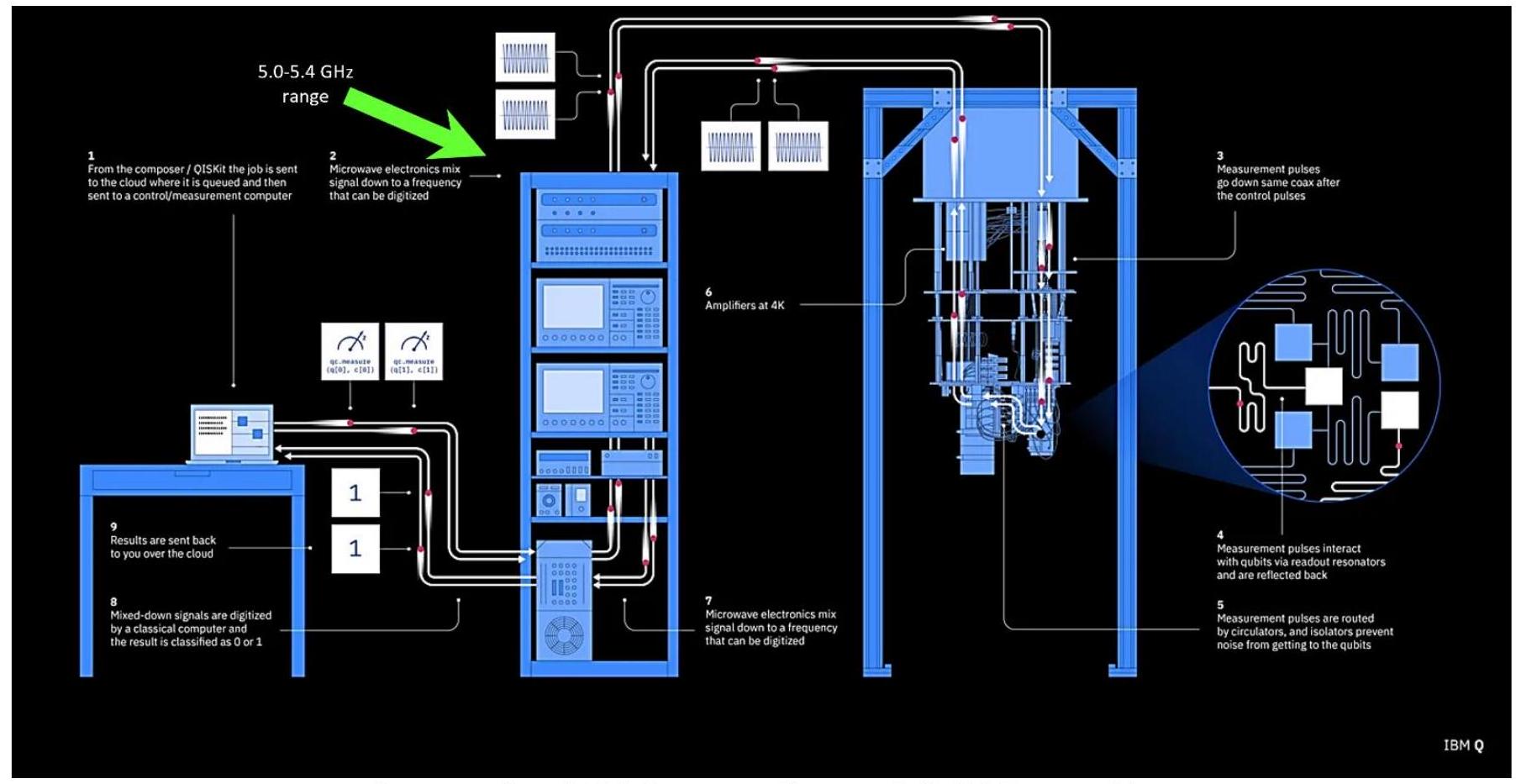
Layout of an IBM Quantum System 1 (IBM Research).
A quantum computing system can be described by the quantum stack, containing levels of abstraction. The software layer exists on the upper level, while the hardware layer is on the lower level. At the very bottom of this hardware level is the quantum chip, which comprises of a quantum processing unit (QPU). One may notice, in nearly every quantum computing platform, the processor comes in some form of a chip. It contains components that can exploit quantum effects depending on the material's physical properties. The overall control and conversion systems vary in size, however. Some can fit inside a desktop machine, while others take up the space of an entire building room, like early vacuum tube-based computers.
The DiVincenzo criteria is a guide that can be used to realize gate-based quantum computation, of which effects like quantum interference, entanglement, and superposition are highly important. Physical quantum bits (qubits) are primary components for making quantum logic gates, along with their controllers, converters, couplers, readout connectors, etc. To build these devices requires materials that are shapeable and can be patterned into useful objects, typically, a few nanometers thick. These are what we call nanoscale thin films. Many materials used in fabricating thin film devices for quantum are compatible with existing semiconductor fabrication tools (i.e., lithography, thin film deposition, and dry etching equipment).
DiVincenzo Criteria:
- Scalable architecture containing well-defined qubits.
- Distinct and reliable qubit state preparation.
- Decoherence times much longer than gate operation times.
- Universal set of quantum gates that perform accurate operations on the qubits.
- Well defined readout capability for each individual qubit.
Physical qubits are a two-level system and can be made of solid-state or non-solid-state devices. This means that the single atoms or clusters of atoms or molecules being used to make a useful qubit can exist in either a solid form of matter or a non-solid (photons, in this case). Devices based on superconducting junctions, quantum dots, nitrogen vacancies, and topological systems are of the solid-state type. Here, solid-state quantum devices will be highlighted. (In the future, we can expect more quantum platforms made of different solid-state materials that are also compatible with the latest manufacturing techniques, so keep this in mind).
In recent decades, nanofabrication techniques have made controllable quantum devices a reality, although quantum devices are not necessarily a sub-field of nanotechnology. It is widely acknowledged that device sizes from 1 to 100 nanometers ( 10 to 1,000 Ångstroms) are of the nanoscale. In this range, it is widely known that quantum effects are more likely to occur and are more observable in measurement. (Measurement is usually performed physically or converted into an electronic signal that can be easily recorded for analysis to confirm quantum behavior). As a result, many fabricated quantum devices are made of nanometer structures, typically in the vertical direction. One can make a quantum device that uses
For nanoscale features, optical (light) microscopes have difficulty in imaging, physically limited by the wavelength of light. Thus, an electron microscope or other specialized imaging system which uses wavelengths shorter than light are needed to properly view nanoscale objects while engineering a device.
The word "lithography" comes from the German word "lithographie," a combination of the ancient Greek words líthos, meaning "stone," and gráphein, meaning "to write." In the context of nanotechnology manufacturing, lithography is referred to as the development of so-called oneand two-dimensional structures. Here, at least one of its dimensions is in the nanometer range. Lithography allows one to copy patterns from computer generated designs onto an underlying substrate with a compatible adhesion layer. (A substrate is a type of supporting foundation, usually a wafer, while an adhesion layer promotes bonding between the substrate and film of interest). There are two sub-categories of lithography: masked and maskless. One may also hear the term direct-write, which refers to maskless exposure techniques. The masked exposure technique is basically like using a stencil, which allows one to draw designs repeatedly onto a surface by guiding a writing source through cut-out patterns.
General lithography is further divided into photolithography, electron-beam lithography, X-ray and extreme ultraviolet lithography, focused ion beam lithography and neutral atom beam lithography, soft lithography, colloidal lithography, nanopattern/ imprinting lithography, scanning (thermal) probe lithography, atomic force microscope lithography, etc. Each method involves energy exposure to a specific area with either the help of beam control systems or a patterned mask.
The two approaches for general manufacturing are called top-down, which involves cutting away pieces of a bulk material, and bottom-up, which involves growing or assembling atoms and molecules into larger structures. These two methods are applied in nanofabrication. Since thin film etching is a top-down process, while thin film growth and nanomolding is a bottom-up process, lithography is considered to be a hybrid method since it can use either or both processes. Nanomanipulation and nanoimprinting are examples of mostly bottom-up fabrication techniques. Dry (physical) etching and wet (chemical) etching methods correlate to anisotropic and isotropic profiles, respectively. (A profile or side profile is referred to as a cross-sectional view).
Vacuum deposition chambers, their support systems, and interfaces can be seen in fabrication laboratories virtually everywhere. The two main types of deposition chambers are physical vapor deposition and chemical vapor deposition. These systems support the growth of material multilayers on sample substrates, such as
Improving nanotechnology manufacturing methods enables innovative approaches for solving quantum hardware problems every day. To develop quantum devices, it usually begins with an idea on paper, where a device circuit or cross-sectional diagram of one eventually will become a real chip. One may choose to hand draw the ideas. Then, once the overall device function is principally understood, it can be translated to a software design application, such as Autodesk AutoCAD. Geometries can be modified and drawn to-scale on the software so that layers of the chip can overlap, interface, or connect with each other as intended. In more complicated designs, the steps can be programmed and automated using layout processing software.
From here, the design can easily be converted into a machine code by exporting specific file formats, with coordinates that a lithography machine can understand. The converted design file creates a virtually marked pathway to guide or control the beam or write head in a lithography machine. However, before it is uploaded for lithography, it should pass inspection for quality assurance and troubleshooting. Afterwards, the final machine code for patterning can be uploaded. From here, a prepared sample containing necessary (thin film) material layers for devices can be loaded for proper lithography alignment and exposure for polymerization.
When the initial lithography step is completed, the sample will be ready for etching, followed by deposition and planarization of required dielectrics, metals, or non-metal layers until the devices are finished and ready for testing. Sometimes, an extra step to add a device to a larger chip architecture or packaging is performed, including wire bonding. In the many pictures of quantum devices and processors you may find by means of the internet or in books, the exposed wire bonds and leads can be seen connecting the chip to its packaging. It is the typical appearance of a finished test sample. For industrial-scale quantum device samples that are being mass manufactured, wire bonded components are sealed within the packaging, like the case with classical semiconductor chips. For high-density quantum chips, the packaging interface may involve bump bonding with superconducting metal that remains malleable under cryogenic conditions, such as indium for example.
Notice that the general process described above is very similar to the scenario for 3D printing or computer numerical control (CNC) machining. (It involves design files that are converted into G-codes, which guide the printer or milling heads to their locations on a printing or milling stage, using
A General Process Flow for Fabricating Quantum Chips Using a Top-Down Method
Part 1:
Idea for Device(s)
Part 2:
Prepare Sample for Lithography
Part 3:
Electrode Contact Deposition
(Note: an inspection process is typically implemented at the end of each step).
If one wanted to visualize the engineering of atoms into nanostructures that can support quantum information systems, below are some ideas for intuition. The entire fabrication process is like preparing a multi-layered bakery item (e.g., cake), which gets sliced up into pieces and sculpted into arbitrary 3D shapes. (In the supplementary images, you can see an example of how a cake is formed into unique shapes by this description). Another analogy for the process of nanofabrication is the stacking of LEGO bricks, which too can be separated into groups of unique shapes. As a metaphor, each individual brick is the representation of an atom, some of which are slightly larger than others, yet still interlinkable overall.
By examining a close-up of atoms through an imaging system that supports atomic resolution modes, one can observe arrangements of dots. These dots displayed on such a microscope (e.g., transmission electron microscope or scanning tunneling microscope) are more like representations of atoms, based on the interaction of electrons around each atom with the beam or probe being used to scan a sample. Although you cannot distinguish between individual electrons or components of the nuclei in each atom being scanned in the microscope, it is possible to measure things like interatomic spacing and crystallinity. In other words, one can choose to inspect nanostructures of fabricated samples using atomic resolution imaging techniques to check on how organized or unorganized its atoms are.
It is useful to combine electron imaging with other surface analysis methods to doublecheck on how well atomic layers will adhere or interface with each other. Diffusion barriers, tunnel barriers, and blockades are also closely inspected using the above-mentioned techniques in solidstate nanostructures. These layers typically exist at device interfaces and serve the purpose of filtering out states or impurities that may move from region to region based on applied heat, voltage, current, field, etc. Therefore, it is worth performing a cross-sectional inspection of the multilayers before patterning and optionally after a prototype chip has been patterned.
In conclusion, nanotechnology is a highly interdisciplinary STEM field that is applicable to quantum technology yet does not contain quantum as a specific sub-category. It is an indispensable tool for realizing the platforms that host quantum information systems and processing. On the other hand, quantum technology as a field does contain a sub-category in hardware that covers nanotechnology and its related applications. This is where quantum chips and devices are discussed. To build the chip hardware at the bottom of the quantum stack requires an understanding of manufacturing at the atomic and nanoscale. Precision control and fine tuning of systems are key ideas of the intersection between both technologies. They can be leveraged to meet the sustainability needs of tomorrow and the distant future.
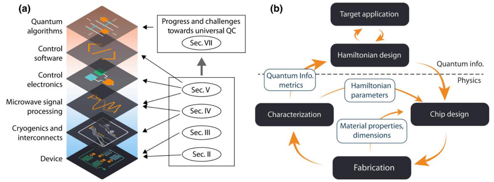
Overview of the Full Quantum Stack vs. the Engineering Cycle of Circuit Quantum Electrodynamics (cQED) Device (Gao at al., PRX Quantum, 2021).
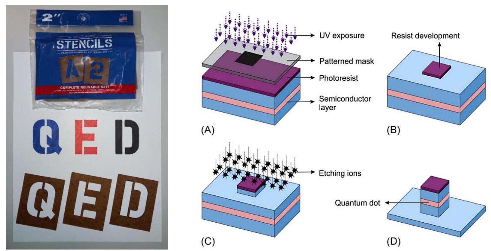
Stencil Cut-Out [Left] vs. Lithography Exposure Mask [Right] (Onri Jay Benally) & (Kumar et al., Synthesis of Inorganic Nanomaterials, 2018).
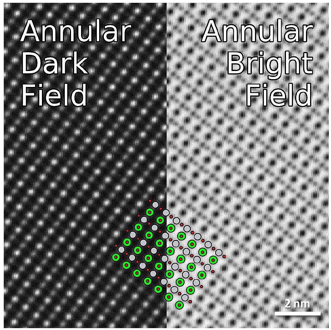
Dark Field & Light Field Images Taken Using a Scanning Transmission Electron Microscope (STEM). Shown is Crystalline Structure of Atoms From a SrTiO3 Thin Film Sample. The Colored Dots Represent Positions of Atoms. Green: Strontium, Red: Oxygen, & Grey: Titanium. (Wikimedia Commons).
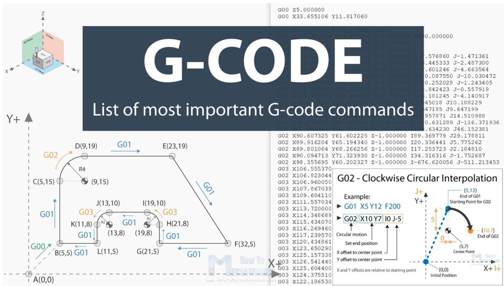
Example of G-Code Used in Both Top-Down and Bottom-Up Manufacturing. Application Includes But is Not Limited to LASER Cutting, CNC Machining, and 3D Printing (howtomechatronics.com).
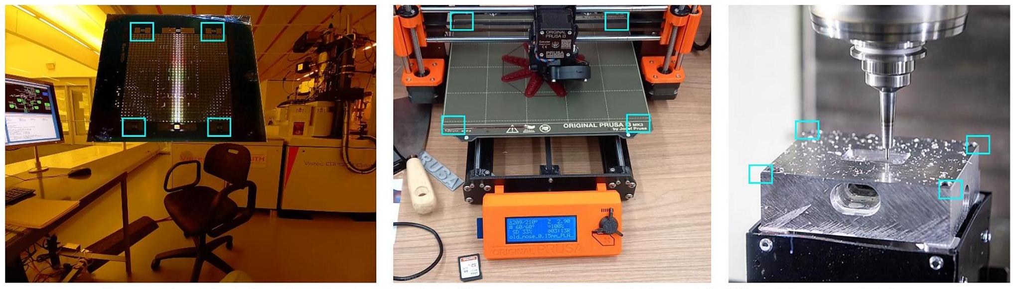
Reference Points Highlighted in Light Blue. Electron-Beam Lithography System [Left], Fused Deposition Modeling 3D Printer [Center], Computer Numerical Control Milling Machine [Right] (Onri Jay Benally) & (Protolabs).
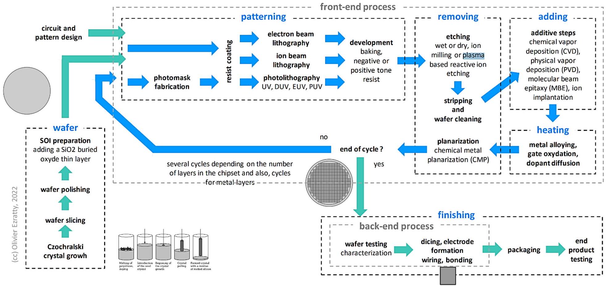
Layout of a General Chipset Manufacturing Process (Ezratty, Understanding Quantum Technologies, 2022).
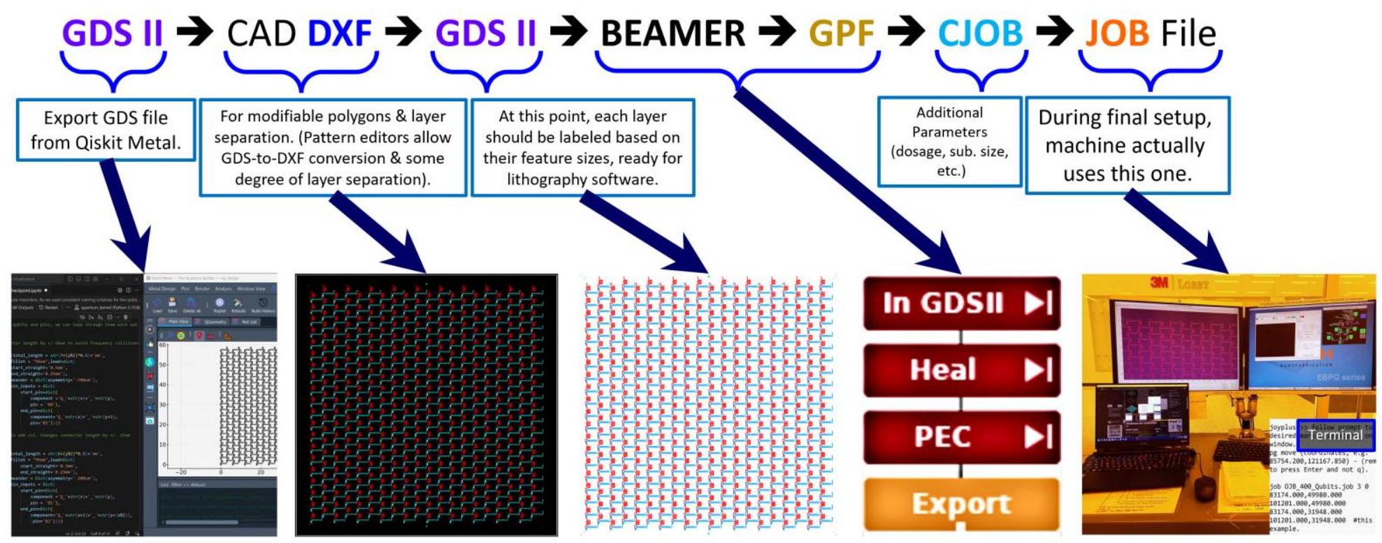
Example of a Quantum Chip Design Process Flow in Preparation for Direct-Write Electron-Beam Lithography Exposure (Onri Jay Benally).
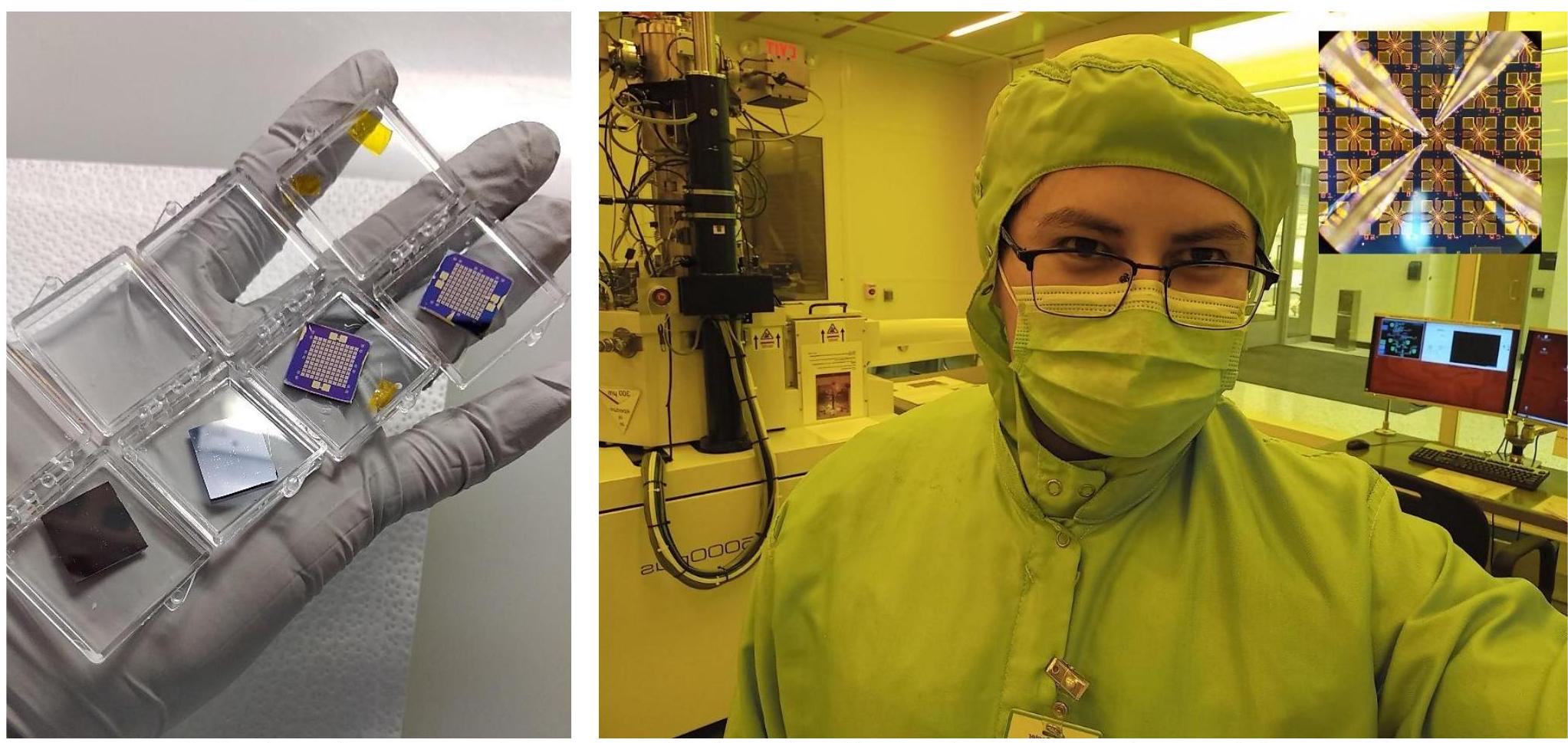
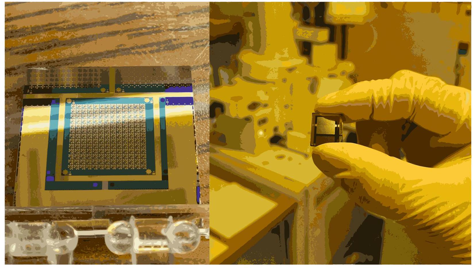
Collection of Unpatterned & Patterned Spintronic Chips [Left]. Self-Portrait Containing a Raith EBPG 5000+ Maskless Electron-Beam Lithography System in the Background [Right] (Onri Jay Benally).
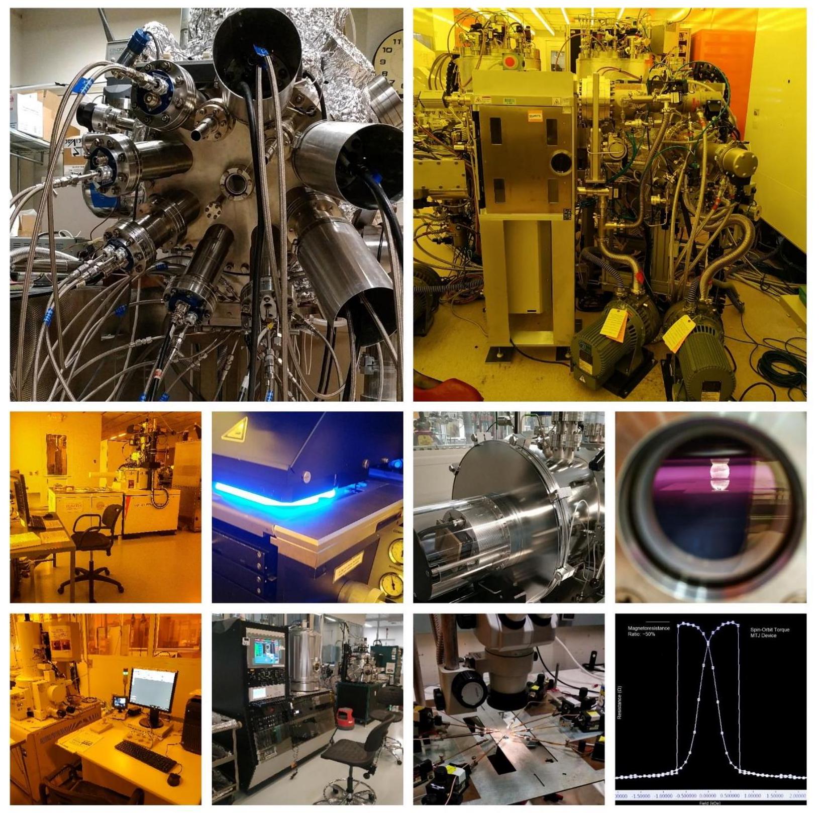
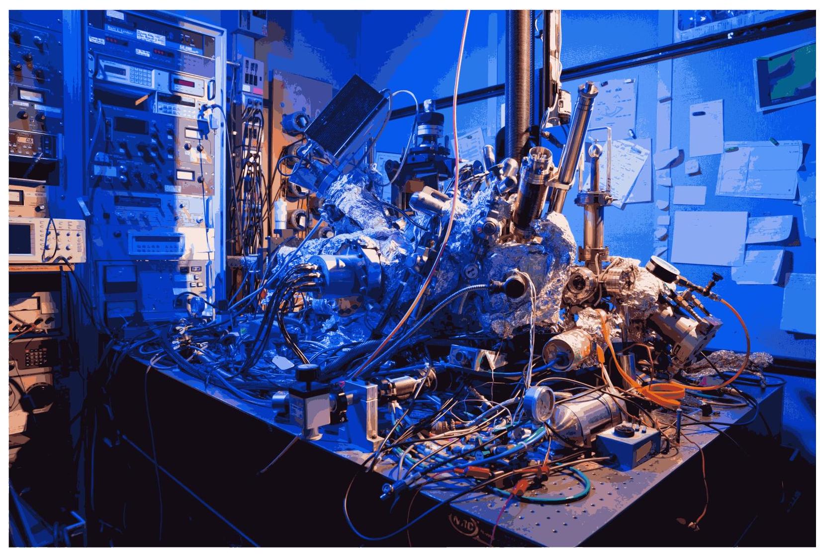
Image Collection of Deposition, Etching, Lithography, and Testing Equipment From the (Nano Magnetism & Quantum Spintronics Lab) & (Minnesota Nano Center), Located at the University of Minnesota-Twin Cities, USA (Onri Jay Benally).
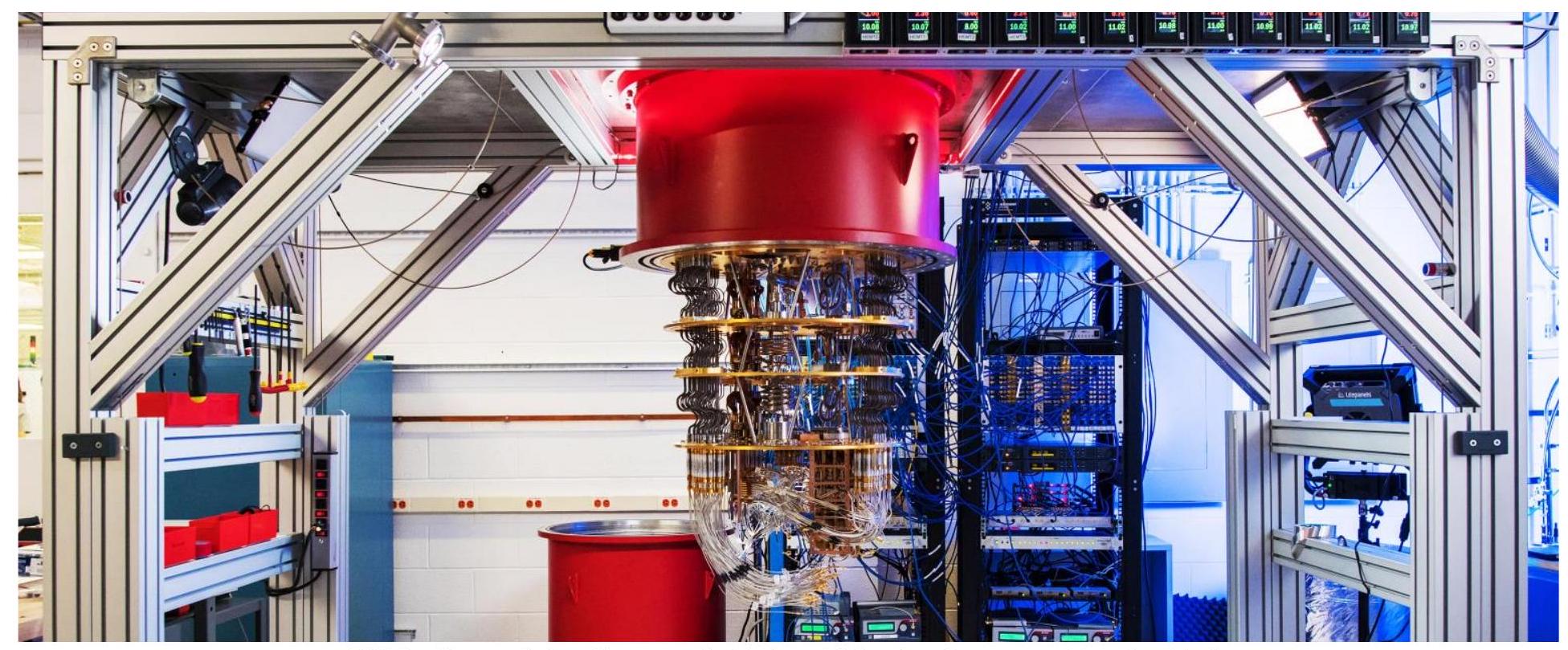
Wide Shot of the Cryogenic Lab within the Quantum Device Lab (Google Quantum AI).
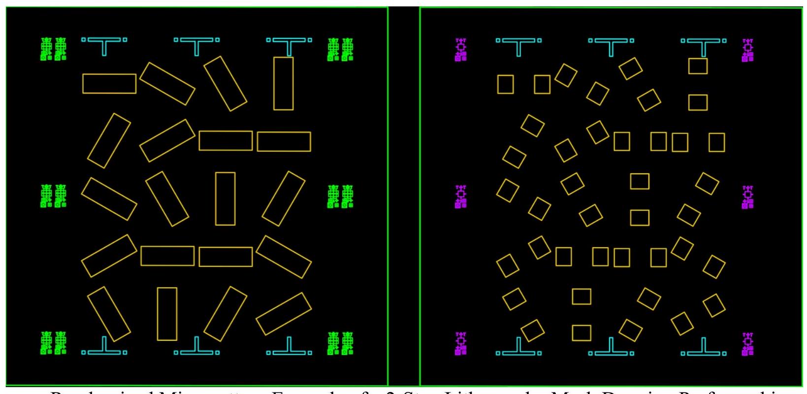
Randomized Micropattern Example of a 2-Step Lithography Mask Drawing Performed in AutoCAD, Containing Rough & Fine Alignment Markers (Onri Jay Benally).
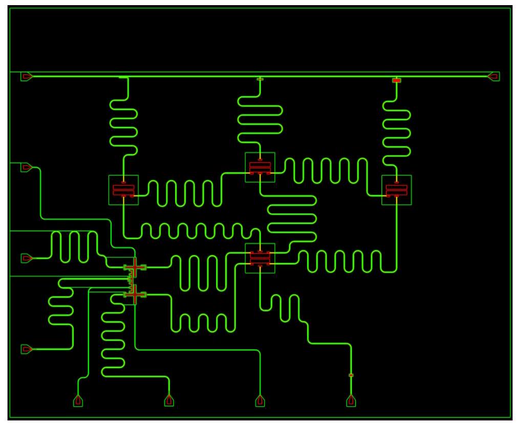
Example of a Multi-Step Lithography Pattern Layout of 6 Superconducting Qubits Converted from an Automated GDS Design File in Qiskit Metal to an AutoCAD Drawing for Inspection (Onri Jay Benally).

Example of a Generic Crossbar Array Layout Shown as an AutoCAD Drawing with Tiny Square Alignment Markers Near the Corners of the Chip (Onri Jay Benally).
Two Fully Fabricated Samples That Employ Electron Spin-Dependent Quantum Tunneling for Efficient Classical Memory in Spintronic Devices Called Spin-Orbit Torque Magnetic Tunnel Junctions (SOT-MTJs). Applications Include but are Not Limited to Magnetic Random-Access Memory, Spin Logic Arrays, & Spin-Based Oscillators (Onri Jay Benally).

Example of a Superconducting Quantum Circuit Layout Prepared in KLayout and Subsequently Rendered with Raytracing Techniques in Blender (Onri Jay Benally).
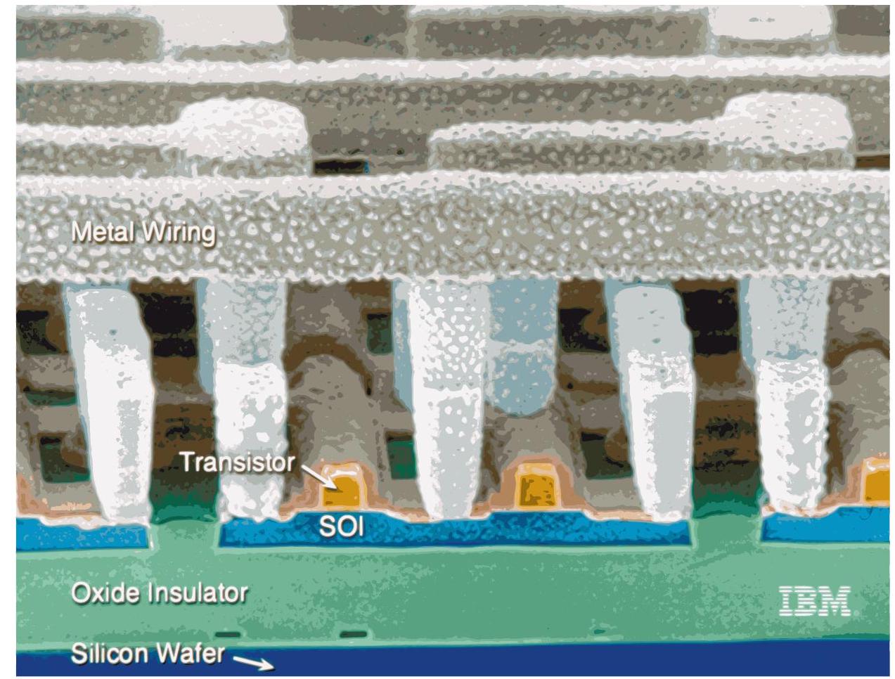
3D Model Cross-Section of An Integrated Device Containing Many Layers Of Deposited, Lithographed, Etched, & Polished Metal (Conductors), Oxides, Nitrides, & Semiconductors (Wikimedia Commons - KAIST).
A Multi-Layered Application Specific Integrated Circuit on Silicon (IBM Research).
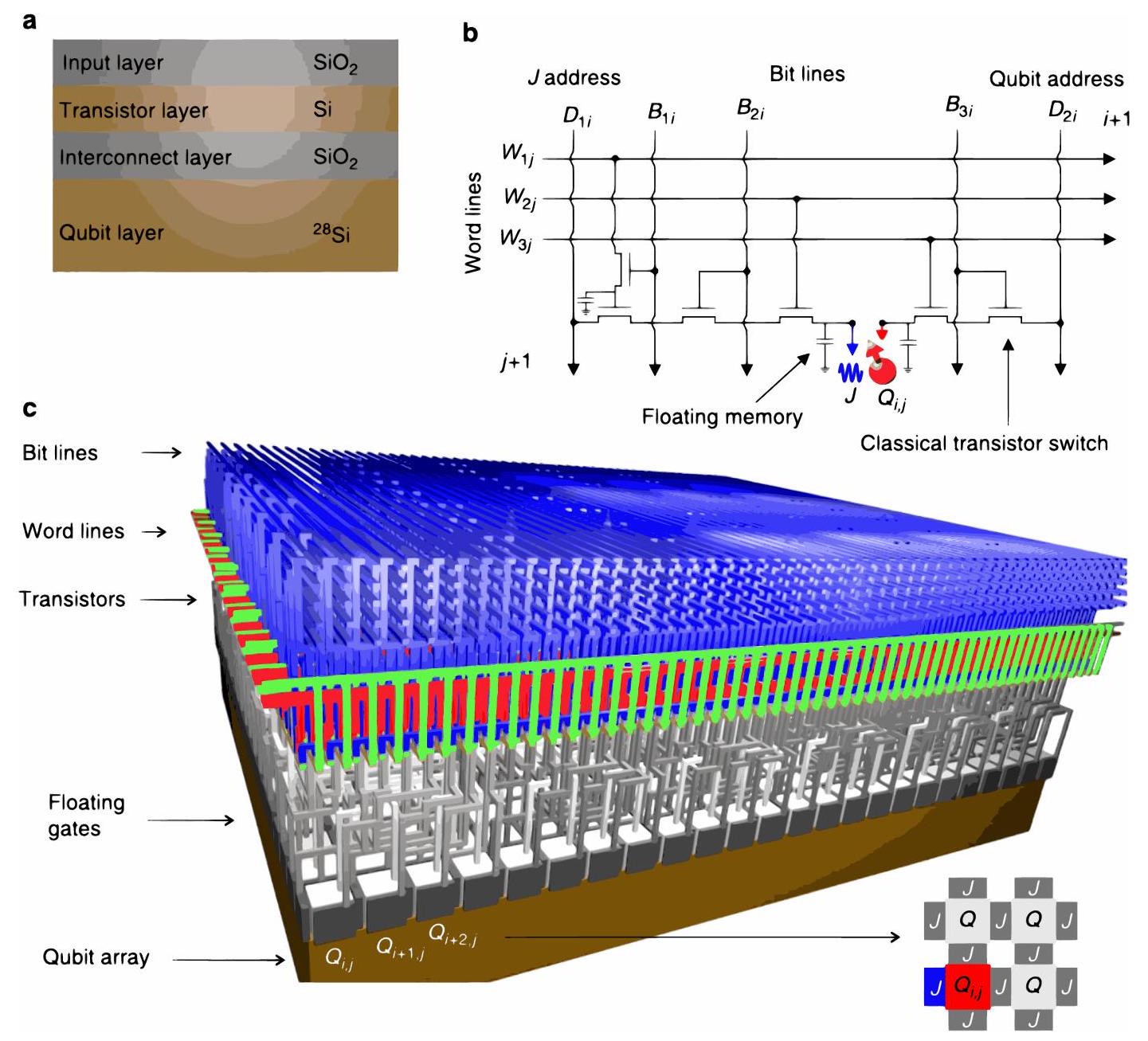
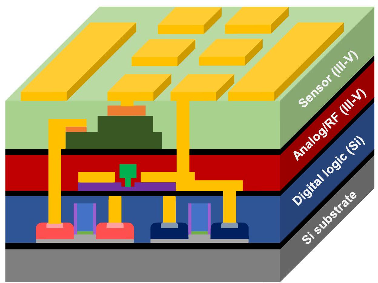
3D Model of a Quantum Integrated Circuit (Veldhorst et al., Nat Commun, 2017).
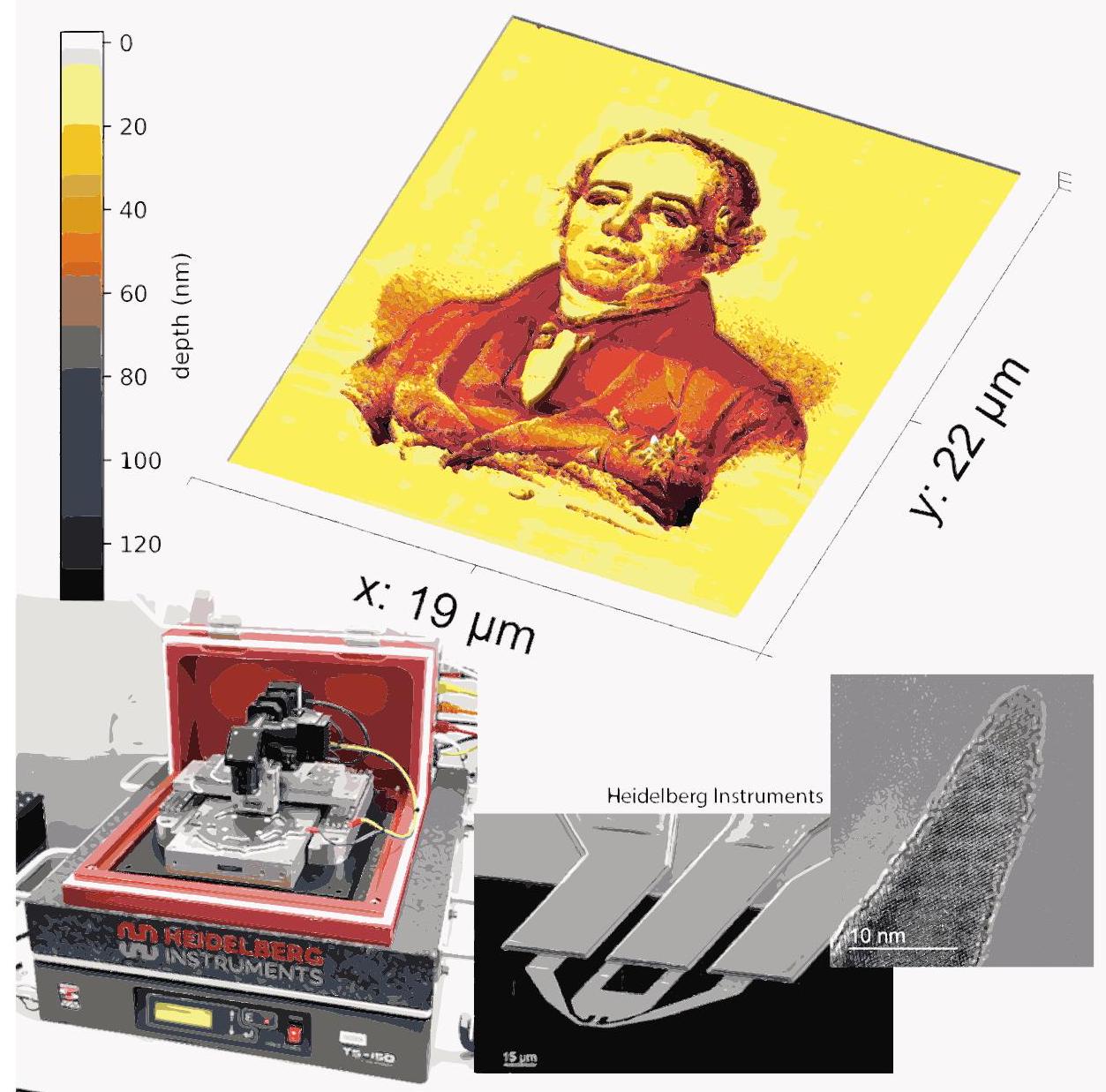
A Portrait of Hans Christian Ørsted That Was Nanopatterned and Subsequently Scanned with an Atomic Force Microscope Probe on the Same Machine, a Heidelberg NanoFrazor
${ }^{\circledR}$ Scanning Thermal Probe Lithography System (Technical University of Denmark-Physics & Heidelberg Instruments).
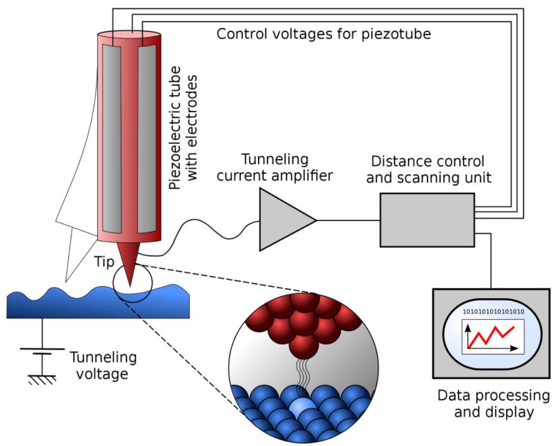
Schematic of a Scanning Tunneling Microscope Used to Image the Topology of a Material or Device Surface at the Atomic Level (Michael Schmid & Grzegorz Pietrzak, CC BY-SA 2.0 at, https://commons.wikimedia.org/w/index.php?curid=89194170).
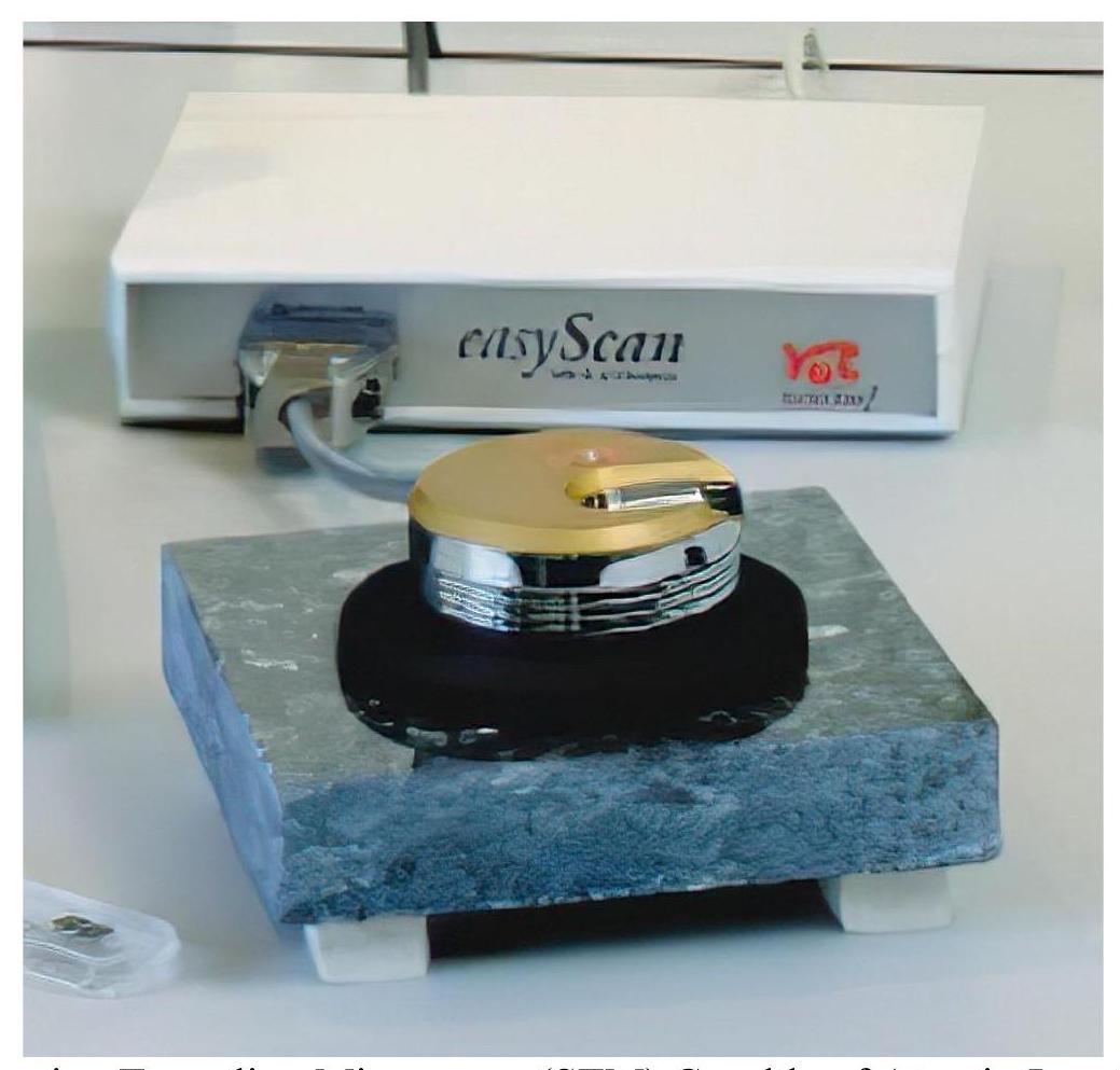
A Desktop Scanning Tunneling Microscope (STM) Capable of Atomic-Level Resolution (Nanosurf).
Setup of a Scanning Tunneling Microscope, Used to Capture Images of Single Atoms or Manipulate Their Position on a Substrate (IBM Research).
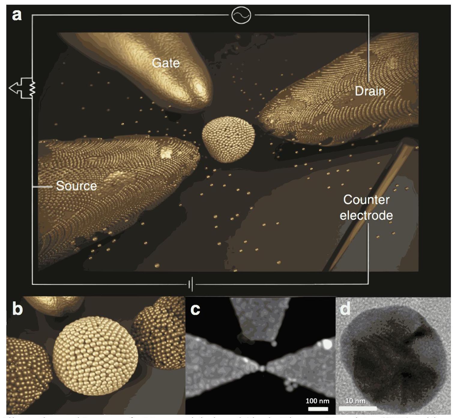
Illustration and Images of a Nanoparticle-based Single-Electron Transistor (SET), with an Arrangement of Source, Drain, and Gate Electrodes. The Last Two Images on the Bottom Show Both Scanning & Transmission Electron Micrographs of the Device (Bitton et al., Nat. Commun., 2017).
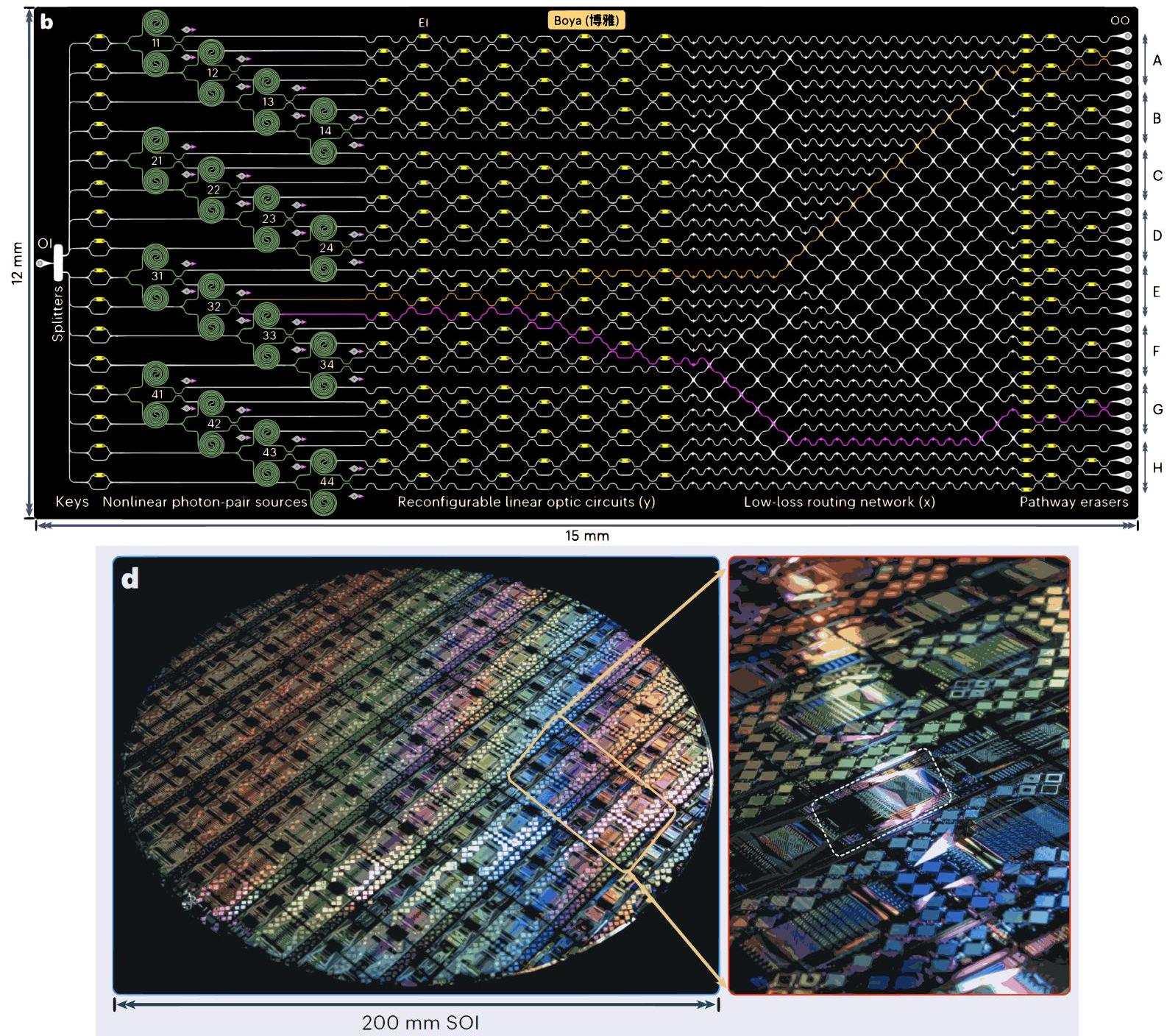
Chip Layout & Wafer Fabricated by Complementary Metal Oxide Semiconductor (CMOS) Processes for Quantum Photonic Circuits (Bao et al., Nature Photonics, 2023).
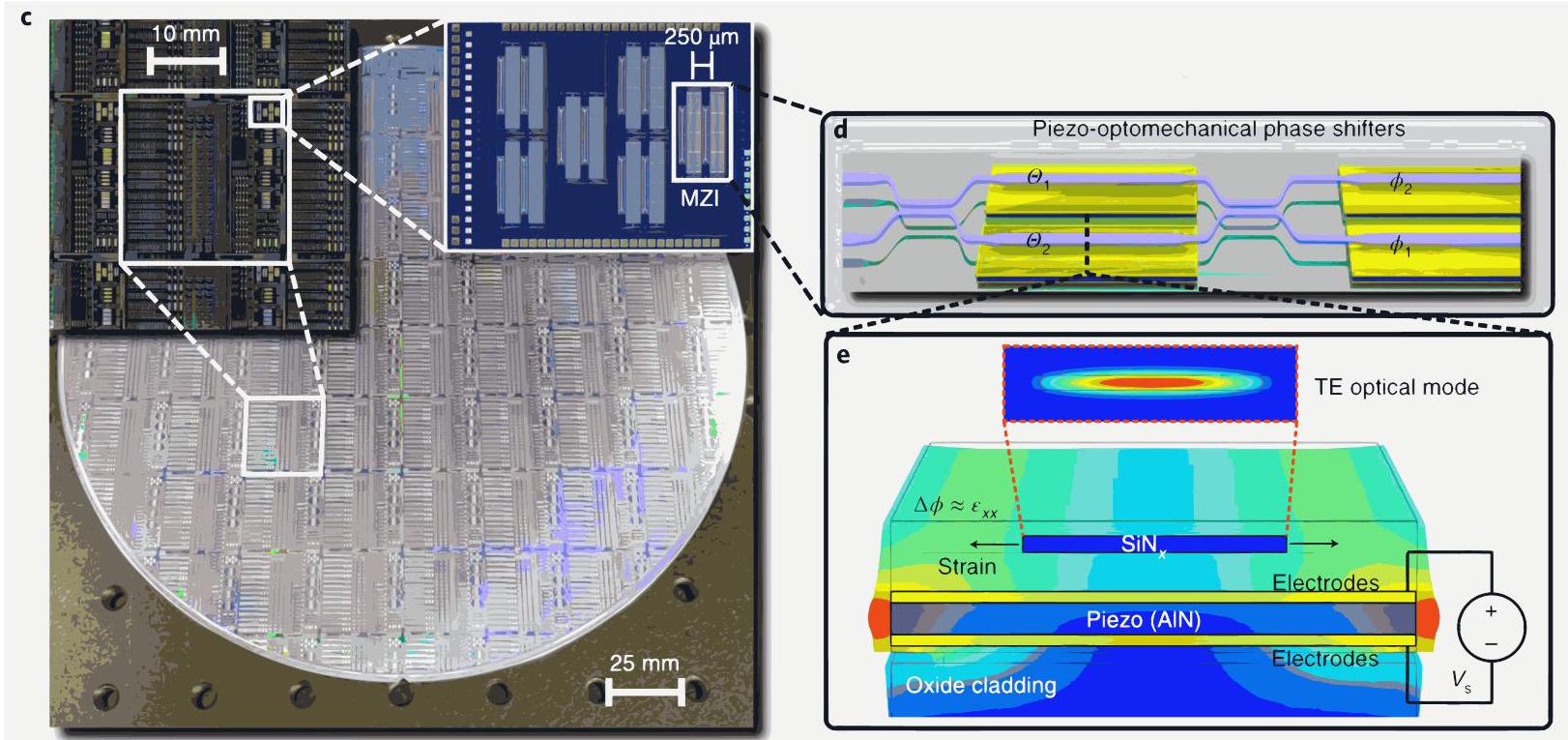
Example of Cascaded Mach-Zehnder Interferometers (MZIs) on a Cryogenically Compatible Quantum Photonics Chip. The Piezo-Optomechanical Components are Designed to Impart Strain on the Optical Waveguides for Chip Control. (Dong et al., Nat. Photon., 2021).
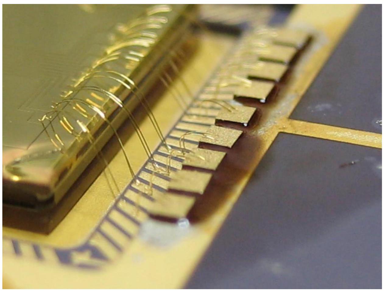
A Close-Up of Gold Wire Bonds on an Oxford Surface Ion Trap Chip (Jeff Sherman, 2009).
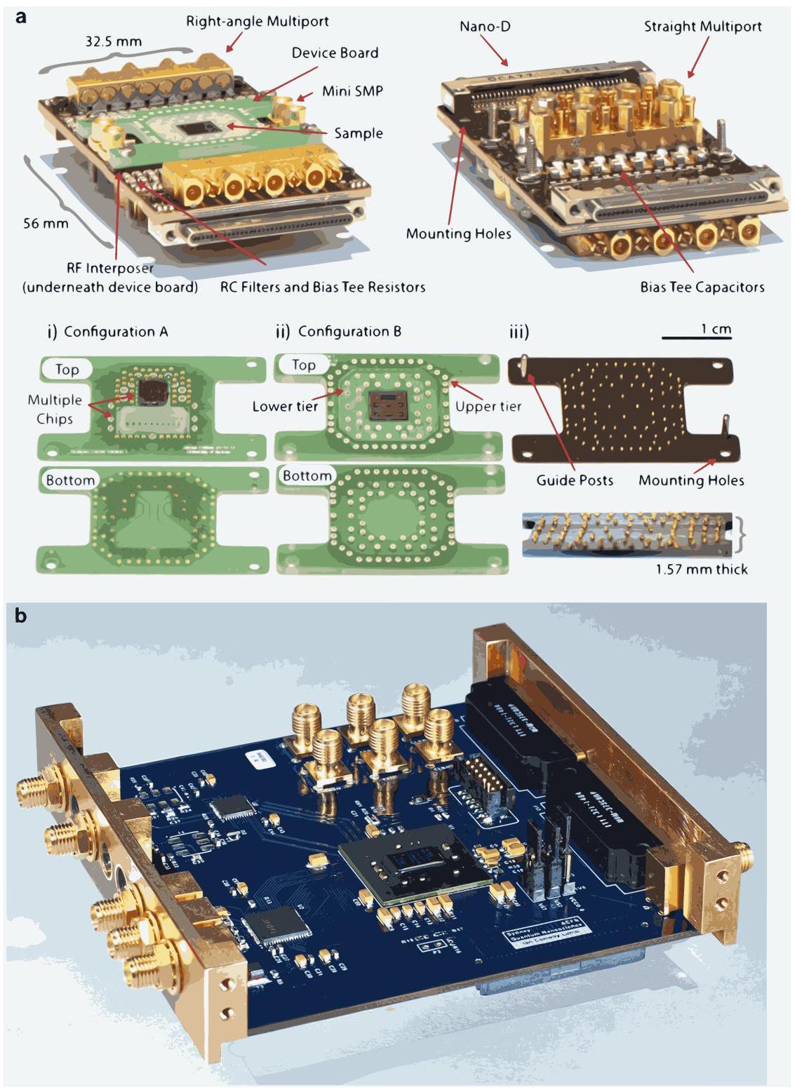
A Modular Cryogenic Circuit Board Containing Digital-To-Analog Converters & Analog-ToDigital Converters, for Interfacing Solid-State Qubits with Commercially Available FieldProgrammable Gate Arrays (FPGAs). Its Purpose is Qubit Readout & Control (Reilly, npj Quantum Inf, 2015).

Example of a Compact Sub-Kelvin Measurement Configuration Using Commercially Available Complementary Metal Oxide (CMOS) Multiplexer (Wuetz et al., npj Quantum Inf, 2020).


