- How many self-dual functions can be made with n variables?
- Total number of combinations:
$2^n$ - Total number of Boolean functions:
$2^{2^n}$ - Total number of self-dual functions:
$2^{2^{n-1}}$
- Total number of combinations:
-
AND Gate:
$A . 0 = 0$ $A . 1 = A$ $A . \bar A = 0$
-
OR Gate:
$A + 0 = A$ $A + 1 = 1$ $A + \bar A = 1$
-
XOR Gate:
$A ⊕ A = 0$ $A ⊕ \bar A = 1$ -
$A ⊕ 0 = A$ // Output is same as input -
$A ⊕ 1 = \bar A$ // Output is inverted -
$A ⊕ A ⊕ A ⊕ A ⊕ A ⊕ A ... n\ times$ :- If
nis even, result$=0$ - If
nis odd, result$=A$
- If
-
NAND Gate: If any 1 of the inputs is 0, output is 1.
-
NOR Gate: If any 1 of the inputs is 1, output is 0.
-
XNOR Gate:
$A ⊙ A = 1$ $A ⊙ \bar A = 0$ -
$A ⊙ 0 = \bar A$ // Output is inverted -
$A ⊙ 1 = A$ // Output is same as input -
$A ⊙ A ⊙ A ⊙ A ⊙ A ⊙ A ... n\ times$ :- If
nis even, result$=1$ - If
nis odd, result$=A$
- If
- For Signed Magniture (SM) & 1's Complement: For n-bits, there are
$2^n$ possible numbers, and the ranges are$-(2^{n-1}-1)$ to$(2^{n-1}-1)$ If Range is
$0$ to$2^n/2 - 1$ , then$2^n/2-1=2^{n}.2^{-1}-1=2^{n-1}-1$ - For 2's Complement: For n-bits, there are
$2^n$ possible numbers, and the ranges are$-(2^{n-1})$ to$(2^{n-1}-1)$ The negative range starts at one less than the previous, while the positive range remains the same.
- Idempotent:
$A.A = A$ - Commutative:
$A.B = B.A$ - Associative:
$(A+B)+C = A+(B+C)$
[1/0 = Doesn't have/has property]
| Gates | Symbol | Idempotent/Closure | Commutative | Associative |
|---|---|---|---|---|
| NOT | ¬ | 0 | NA | NA |
| AND | . | 1 | 1 | 1 |
| OR | + | 1 | 1 | 1 |
| NAND | ↑ | 0 | 1 | 0 |
| NOR | ↓ | 0 | 1 | 0 |
| XOR | ⊕ | 0 | 1 | 1 |
| XNOR | ⊙ | 0 | 1 | 1 |
- Basic Gates: The most basic of all: AND, OR, NOT
- Universal Gates: Combination of basic gates, can be used to make any other gate: NAND (AND + NOT), NOR (OR + NOT)
- Arithmetic Gates: Used to perform arithmetic operations: XOR, XNOR
- Evaluation:
- AND: 1 if both A & B are 1, otherwise 0.
- OR: 1 if either of A or B are 1, otherwise 0.
- NOR: Negation of OR, 1 if A OR B is 0, otherwise 0.
- NAND: Negation or AND, 1 if A AND B is 0, otherwise 0.
- XOR: 1 if both A & B are different, otherwise 0.
- XNOR: 1 if both A & B are same, otherwise 0.

Image taken from here
| A | B | AND | OR | NOR | NAND | XOR | XNOR |
|---|---|---|---|---|---|---|---|
| A | B | A.B | A+B | ¬(A.B) | ¬(A+B) | A ⊕ B | A ⊙ B |
| 0 | 0 | 0 | 0 | 1 | 1 | 0 | 1 |
| 0 | 1 | 0 | 1 | 1 | 0 | 1 | 0 |
| 1 | 0 | 0 | 1 | 1 | 0 | 1 | 0 |
| 1 | 1 | 1 | 1 | 0 | 0 | 0 | 1 |
- Inputs:
$A$ ,$B$ | Outputs:$Y$ - If any 1 of the inputs is 0, output is 0.
- Truth-Table:
A B Y 0 0 0 0 1 0 1 0 0 1 1 1
- Inputs:
$A$ ,$B$ | Outputs:$Y$ - If any 1 of the inputs is 1, output is 1.
- Truth-Table:
A B Y 0 0 0 0 1 1 1 0 1 1 1 1
- Inputs:
$A$ | Outputs:$Y$ - If any 1 of the inputs is 1, output is 1.
- Truth-Table:
A Y 0 1 1 0
- Inputs:
$A$ ,$B$ | Outputs:$Y$ - If any 1 of the inputs is 0, output is 1.
- Truth-Table:
A B Y 0 0 1 0 1 1 1 0 1 1 1 0
-
Inputs:
$A$ ,$B$ | Outputs:$Y$ -
If any 1 of the inputs is 1, output is 0.
-
Truth-Table:
A B Y 0 0 1 0 1 0 1 0 0 1 1 0 -
To implement OR gate, we need 3 NAND gates or 2 NOR gates.
Gates NAND NOR NOT 1 1 AND 2 3 OR 3 2 XOR 4 5 XNOR 5 4
- If 2 inputs are A & B, A ⊕ B =
$A \bar B + \bar AB$ - If both inputs are same, output will be
0, otherwise1. - In a K-Map, if the diagonals are covered with 1, we can take XOR of the variables.
- Truth Table:
A B Y 0 0 0 0 1 1 1 0 1 1 1 0 - Examples:
$A ⊕ A = 0$ $A ⊕ \bar A = 1$ -
$A ⊕ 0 = A$ (Exchange property: In(i), put0in LHS &Ain RHS) -
$A ⊕ 1 = \bar A$ (Exchange property: In(ii), put1in LHS &$\bar A$in RHS) -
$A ⊕ A ⊕ A ⊕ A ⊕ A ⊕ A ... n\ times$ :- If
nis even (for example$n=4$ ),$A ⊕ A ⊕ A ⊕ A = 0 ⊕ 0 = 0$ - If
nis odd (for example$n=3$ ),$A ⊕ A ⊕ A = 0 ⊕ A = A$
- If
- XOR Gate can be used as buffer/inverter: Since
$A ⊕ 0 = A$ &$A ⊕ 1 = \bar A$ , we can give an inputA& use the 2nd input as control. If the control is 0, output is same as input, otherwise output is inverted.
- Negation (¬) of XOR Gate.
- If 2 inputs are A & B, A ⊙ B =
$AB + \bar A \bar B$ - If both inputs are same, output will be
1, otherwise0. - Truth Table:
A B Y 0 0 1 0 1 0 1 0 0 1 1 1 - Examples:
$A ⊙ A = 1$ $A ⊙ \bar A = 0$ -
$A ⊙ 0 = \bar A$ (Exchange property: In(i), put0in LHS &Ain RHS) -
$A ⊙ 1 = A$ (Exchange property: In(ii), put1in LHS &$\bar A$in RHS) -
$A ⊙ A ⊙ A ⊙ A ⊙ A ⊙ A ... n\ times$ :- If
nis even (for example$n=4$ ),$A ⊙ A ⊙ A ⊙ A = 1 ⊙ 1 = 1$ - If
nis odd (for example$n=3$ ),$A ⊙ A ⊙ A = 1 ⊕ A = A$
- If
- XNOR Gate can be used as buffer/inverter: Since
$A ⊙ 0 = \bar A$ &$A ⊙ 1 = A$ , we can give an inputA& use the 2nd input as control. If the control is 1, output is same as input, otherwise output is inverted.
-
SoP need not contain all the literals, but in Canonical form, each product term should contain all literals, be it in complemented or un-complemented form.
-
The product terms themselves are called the min-terms.
-
Sum of all min-terms for which output
$f= 1$ , is called Canonical Sum of Product, or disjunctive normal form. -
Truth Table:
x y z Decimel f 0 0 0 0 0 0 0 1 1 1 0 1 0 2 0 0 1 1 3 1 1 0 0 4 0 1 0 1 5 1 1 1 0 6 0 1 1 1 7 1 - If
$x=0$ , we write$\bar x$ , otherwise we write$x$ . - So, SoP ie
$f(1) = \bar x \bar y z + \bar x y z + x \bar y z + xyz$ - We can also write it as
$∑m(1,3,5,7)$ or$∑(m$ 1$+m$ 3$+m$ 5$+m$ 7$)$ .
- If
| Source | Destination |
|---|---|
| OR | AND |
| . | + |
| NOT | keep as-is |
| XOR | XNOR |
| NAND | NOR |
| 0 | 1 |
| Variable | keep as-is |
-
Complement: Has all properties of the Duality Theorem, and we complement the variables in addition.
$A\ <->\ \bar A$ $\bar A\ <->\ A$
-
Example 0:
$XOR = \bar A B + A \bar B$ $(\bar A + B) . (A + \bar B)$ $\bar A A + AB + \bar A \bar B + B \bar B$ -
$(AB + \bar A \bar B) = XNOR$ [Duality] -
$(\bar A \bar B + A B)$ [Complement]
-
Example 1:
$(AB \bar C)+(\bar ABC) + (ABC)$ -
$(A+B+ \bar C).(\bar A + B+C).(A+B+C)$ [Duality] -
$(\bar A + \bar B + C).(A + \bar B + \bar C).(\bar A + \bar B + \bar C)$ [Complement]
-
-
Example 2:
$(XYZ)+(\bar X Y \bar Z)+(\bar Y Z) = 1$ -
$(X+Y+Z).(\bar X + Y + \bar Z).(\bar Y + Z) = 0$ [Duality] -
$(\bar X+ \bar Y + \bar Z).(X + \bar Y + Z).(Y + \bar Z) = 0$ [Complement]
-
-
Example 3, demonstrating self-dual equation:
$XY+YZ+XZ)$ $(X+Y).(Y+Z).(X+Z)$ -
$(XY+XZ+Y+YZ).(X+Z)$ #Y.Ycan be written asY $(Y[X+1+YZ]+XZ).(X+Z)$ -
$(Y+XZ)(X+Z)$ # 1 added with anything will result in1, soX+1+YZis resolved to1. -
$XY+YZ+XZ+XZ$ #XXZ=XZ&XZZ=XZ -
$XY+YZ+XZ$ #XZ+XZ=XZ - This kind of equation is called a self-dual equation. In other words, the output is the same as input in such an equation.
-
Example 4: How many self-dual functions can be made with 1 variable?
- Total number of combinations: 2, ie A can be either 0 or 1
- Total number of Boolean functions: 4, ie
$0,1, A$ or$\bar A$ - Total number of self-dual functions: 2 (out of
$0,A,\bar A,1$ , only$A, \bar A$ are self-dual)A $f_1$ $f_2$ $f_3$ $f_4$ 0 0 0 1 1 1 0 1 0 1 Result 0 $A$ $\bar A$ 1
-
Example 5: How many self-dual functions can be made with 2 variables?
- Total number of combinations: 4, ie A can be either 0 or 1 & B can also be either 0 or 1
- Total number of Boolean functions: 16.
- Total number of self-dual functions: 4, ie only
$A, \bar A, B, \bar B$ are self-dual out of all functions.A B $f_1$ $f_2$ $f_3$ $f_4$ $f_5$ $f_6$ $f_7$ $f_8$ $f_9$ $f_{10}$ $f_{11}$ $f_{12}$ $f_{13}$ $f_{14}$ $f_{15}$ $f_{16}$ 0 0 0 0 0 0 0 0 0 0 1 1 1 1 1 1 1 1 0 1 0 0 0 0 1 1 1 1 0 0 0 0 1 1 1 1 1 0 0 0 1 1 0 0 1 1 0 0 1 1 0 0 1 1 1 1 0 1 0 1 0 1 0 1 0 1 0 1 0 1 0 1
-
aka Karnaugh Map
-
A K-Map is used to graphically represent & minimize boolean expressions.
-
For a boolean expression of
nvariables, number of cells needed in K-Map is$2^{n}$ . -
K-Map is based on Grey code (unit distance code). We can't change more than 1 bit in a single step.
-
Prime Implicants: Min-terms which have a
1in them. -
Essential Prime Implicants: Min-terms which have a
1in them, which is also not shared with other pairs. -
There are 3 types of input values,
0,1,d,x (don't care). -
Steps:
- We generate the K-Map.
- We find the pairs. They contain 1 mandatorily. We may take
diedon't careif needed, otherwise we ignore them. While pairing elements, we first try to find the biggest pair possible (16 elements in a K-Map of 16 elements). Then, we gradually decrease the pair size. - We find the min-terms. Min-terms consist of variables which are same/common for all elements of the pair.
-
Example: Generate a K-Map for
$(A,B,C)$ &$(A,B,C,D)$ -
Detailed versions (the cell values denote the decimel representation of the positions):
-
2 variables,
$AB$ :$↓A\ |\ B→$ $\bar B_{(0)}$ $B_{(1)}$ $\bar A_{(0)}$ $0_{(00)}$ $1_{(01)}$ $A_{(1)}$ $2_{(10)}$ $3_{(11)}$ -
3 variables,
$ABC$ :$↓A\ |\ BC→$ $\bar B \bar C_{(00)}$ $\bar B C_{(01)}$ $B C_{(11)}$ $B \bar C_{(10)}$ $\bar A_{(0)}$ $0_{(000)}$ $1_{(001)}$ $3_{(011)}$ $2_{(010)}$ $A_{(1)}$ $4_{(100)}$ $5_{(101)}$ $7_{(111)}$ $6_{(110)}$ -
4 variables,
$ABCD$ :$↓AB\ |\ CD→$ $\bar C \bar D_{(00)}$ $\bar C D_{(01)}$ $C D_{(11)}$ $C \bar D_{(10)}$ $\bar A \bar B_{(00)}$ $0_{(0000)}$ $1_{(0001)}$ $3_{(0011)}$ $2_{(0010)}$ $\bar A B_{(01)}$ $4_{(0100)}$ $5_{(0101)}$ $7_{(0111)}$ $6_{(0110)}$ $AB_{(11)}$ $12_{(1100)}$ $13_{(1101)}$ $15_{(1111)}$ $14_{(1110)}$ $A \bar B_{(10)}$ $8_{(1000)}$ $9_{(1001)}$ $11_{(1011)}$ $10_{(1010)}$
-
-
Simplified versions & templates:
-
2 variables,
$AB$ :$↓A\ |\ B→$ $\bar B$ $B$ $\bar A$ $null_{(0)}$ $null_{(1)}$ $A$ $null_{(2)}$ $null_{(3)}$ -
3 variables,
$ABC$ :$↓A\ |\ BC→$ $\bar B \bar C$ $\bar B C$ $B C$ $B \bar C$ $\bar A$ $null_{(0)}$ $null_{(1)}$ $null_{(3)}$ $null_{(2)}$ $A$ $null_{(4)}$ $null_{(5)}$ $null_{(7)}$ $null_{(6)}$ -
4 variables,
$ABCD$ :$↓AB\ |\ CD→$ $\bar C \bar D_{(00)}$ $\bar C D_{(01)}$ $C D_{(11)}$ $C \bar D_{(10)}$ $\bar A \bar B_{(00)}$ $null_{(0)}$ $null_{(1)}$ $null_{(3)}$ $null_{(2)}$ $\bar A B_{(01)}$ $null_{(4)}$ $null_{(5)}$ $null_{(7)}$ $null_{(6)}$ $AB_{(11)}$ $null_{(12)}$ $null_{(13)}$ $null_{(15)}$ $null_{(14)}$ $A \bar B_{(10)}$ $null_{(8)}$ $null_{(9)}$ $null_{(11)}$ $null_{(10)}$
-
-
-
Example 1:
$f(A,B)=\sum (2,3)$ - Method 1, by directly solving the equation:
A B $f$ 0 0 0 0 1 0 1 0 1 1 1 1 - As per the question,
$f=1$ for index 2 & 3 (within 0-3). - The resultant equation is:
$A \bar B + A B = A(\bar B + B) = A.1 = A$
- As per the question,
- Method 2, using K-Map:
null $\bar B$ $B$ $\bar A$ $0_{(0)}$ $0_{(1)}$ $A$ $1_{(2)}$ $1_{(3)}$ - Pairs: (2) & (3). Output:
$A$
- Pairs: (2) & (3). Output:
- Method 1, by directly solving the equation:
-
Example 2:
$\sum m(0,2,5,7,9,11)+d(3,8,10,12,14)$ $↓PQ\ |\ RS→$ $\bar R \bar S_{(00)}$ $\bar R S_{(01)}$ $R S_{(11)}$ $R \bar S_{(10)}$ $\bar P \bar Q_{(00)}$ $1_{(0)}$ $null_{(1)}$ $d_{(3)}$ $1_{(2)}$ $\bar P Q_{(01)}$ $null_{(4)}$ $1_{(5)}$ $1_{(7)}$ $null_{(6)}$ $PQ_{(11)}$ $d_{(12)}$ $null_{(13)}$ $null_{(15)}$ $d_{(14)}$ $P \bar Q_{(10)}$ $d_{(8)}$ $1_{(9)}$ $1_{(11)}$ $d_{(10)}$ - Pairs:
${8,9,11,10},{0,2,8,10},{5,7}$ - Min-Terms: 4 ie
$P \bar Q, \bar Q \bar S, \bar P Q S, \bar P \bar Q \bar S$ - Essential Prime Implicants: 3 ie
$P \bar Q, \bar Q \bar S,\bar P Q S$
- Pairs:
-
Example 3:
$\sum m(5,11,13,14,15)$ $↓AB\ |\ CD→$ $\bar C \bar D_{(00)}$ $\bar C D_{(01)}$ $C D_{(11)}$ $C \bar D_{(10)}$ $\bar A \bar B_{(00)}$ $null_{(0)}$ $null_{(1)}$ $null_{(3)}$ $null_{(2)}$ $\bar A B_{(01)}$ $null_{(4)}$ $1_{(5)}$ $null_{(7)}$ $null_{(6)}$ $AB_{(11)}$ $null_{(12)}$ $1_{(13)}$ $1_{(15)}$ $1_{(14)}$ $A \bar B_{(10)}$ $null_{(8)}$ $null_{(9)}$ $1_{(11)}$ $null_{(10)}$ - Pairs:
${5,13},{13,15},{15,14},{15,11}$ - Prime Implicants: 4 ie
$B \bar C D, ABD, ABC, ACD$ - Essential Prime Implicants: 3 ie
$B \bar C D, ABC, ACD$
- Pairs:
- Adds 2 bits
- Inputs: 2 | Outputs: 2
- Sum (Least Significant Bit [LSB]):
$x⊕y$ - Carry (Most Significant Bit [MSB]):
$xy$ - Truth Table:
X Y Sum Carry 0 0 0 0 0 1 1 0 1 0 1 0 1 1 0 1 - Min-terms:
- Sum:
$\bar x y, x \bar y=x⊕y$ (In K-Map, diagonals are filled with 1) - Carry:
$xy$
- Sum:
- Circuit Diagram:
- Sum:
$\bar x y + x \bar y$ | Carry:$xy$ 
- Sum:
$x⊕y$ | Carry:$xy$ 
- Sum:


- Adds 3 bits
- Inputs: 3 | Outputs: 2
- 2 Half-Adders = Full-Adder
- Sum:
$x⊕y⊕z$ - Carry:
$xy+yz+zx=(x⊕y)z+xy$ - Truth Table:
x y z( $c_{in})$ sum $c_{out}$ 0 0 0 0 0 0 0 1 1 0 0 1 0 1 0 0 1 1 0 1 1 0 0 1 0 1 0 1 0 1 1 1 0 0 1 1 1 1 1 1 - Min-Terms:
- Sum:
$\sum{(m_1,m_2,m_4,m_7)} = x⊕y⊕z$ $↓x\ |\ yz→$ $\bar y \bar z$ $\bar y z$ $y z$ $y \bar z$ $\bar x$ $null_{(0)}$ $1_{(1)}$ $null_{(3)}$ $1_{(2)}$ $x$ $1_{(4)}$ $null_{(5)}$ $1_{(7)}$ $null_{(6)}$ - Diagonals are filled with 1.
- Carry:
$\sum{(m_3,m_5,m_6,m_7)}= xy+yz+xz=(x⊕y)z+xy$ $↓x\ |\ yz→$ $\bar y \bar z$ $\bar y z$ $y z$ $y \bar z$ $\bar x$ $null_{(0)}$ $null_{(1)}$ $1_{(3)}$ $null_{(2)}$ $x$ $null_{(4)}$ $1_{(5)}$ $1_{(7)}$ $1_{(6)}$ - Pairs:
$y z,xz,xy=xy+yz+xz$
- Pairs:
- Sum:
- Circuit Diagram:
- Sum:
$x⊕y⊕z$ | Carry:$(x⊕y)z+xy$ 
- Sum:

-
Subtracts 2 bits
-
Inputs: 2 | Outputs: 2
-
Subtraction (Least Significant Bit [LSB]):
$x⊕y$ -
Borrow (Most Significant Bit [MSB]):
$\bar xy$ -
Truth Table:
x y sub $b_{out}$ 0 0 0 0 0 1 1 1 1 0 1 0 1 1 0 0 -
When subtracting
$1$ from$0$ , first we have to borrow$1$ . So,$0$ becomes$10$ , and$10-1=1$ , with borrow$1$ . -
Min-terms:
- Sub:
$\bar x y, x \bar y=x⊕y$ - Borrow:
$\bar xy$
- Sub:
-
Circuit Diagram:
- Sub:
$x⊕y$ | Borrow:$\bar xy$ 
- Sub:

- Subtracts 3 bits
- Inputs: 3 | Outputs: 2
- Sub:
$x⊕y⊕z$ - Borrow:
$\bar x y + yz + \bar xz$ - Truth Table:
x y z( $c_{in})$ sub $c_{out}$ 0 0 0 0 0 0 0 1 1 0 0 1 0 1 0 0 1 1 0 1 1 0 0 1 0 1 0 1 0 1 1 1 0 0 1 1 1 1 1 1 - Min-Terms:
- Sub:
$\sum{(m_1,m_2,m_4,m_7)} = x⊕y⊕z$ $↓x\ |\ yz→$ $\bar y \bar z$ $\bar y z$ $y z$ $y \bar z$ $\bar x$ $null_{(0)}$ $1_{(1)}$ $null_{(3)}$ $1_{(2)}$ $x$ $1_{(4)}$ $null_{(5)}$ $1_{(7)}$ $null_{(6)}$ - Diagonals are filled with 1.
- Borrow:
$\sum{(m_1,m_3,m_2,m_7)}=\bar xz+ \bar x y + yz$ $↓x\ |\ yz→$ $\bar y \bar z$ $\bar y z$ $y z$ $y \bar z$ $\bar x$ $null_{(0)}$ $1_{(1)}$ $1_{(3)}$ $1_{(2)}$ $x$ $null_{(4)}$ $null_{(5)}$ $1_{(7)}$ $null_{(6)}$ - Pairs:
$\bar xz, \bar x y, yz$
- Pairs:
- Sub:
- Circuit Diagram:
- Sub:
$x⊕y⊕z$ | Borrow:$\bar xz+ \bar x y + yz$ 
- Sub:

- It is a Combinational circuit that has
$n$ input lines and$1$ output line. - It is an electronic switch that connects 1 of the
ninputs to an output. - Select lines are used to select the input. If the number of inputs is
$n$ and ($n=2^k$ ), the number of select lines will be$k$ . - Multiplexers are functionally complete, which means we can design any circuit using them.
- We will prove that we can make AND, OR, and NOT gates using Multiplexers. If we can make these basic gates, we can also make NAND & NOR gates after this, which are Universal Gates.
- We will use a 2:1 Multiplexer for proving this.
- Inputs:
$A$ ,$B$ - AND Gate:
- Truth Table of AND Gate:
A B O/P 0 0 0 0 1 0 1 0 0 1 1 1 - Min-Terms:
$f=AB$ - Let's give B as select-line.
$B$ Value Input $\bar B$ $0$ $I_1$ $B$ $1$ $I_2$ -
$I_1=0$ , because$0 . B =0$ -
$I_2=A$ , because$A . B = AB$ - Result:
$0 \bar B + A B = AB$
- Truth Table of AND Gate:
- OR Gate:
- Truth Table of OR Gate:
A B O/P 0 0 0 0 1 1 1 0 1 1 1 1 - Min-Terms:
$f=B + A \bar B$ $\bar A B + A \bar B + A B$ $B(\bar A + A) + A \bar B$ -
$B + A \bar B$ // check formula
- Let's give B as select-line.
$B$ Value Input $\bar B$ $0$ $I_1$ $B$ $1$ $I_2$ -
$I_1=A$ , because$A . \bar B = A \bar B$ -
$I_2=1$ , because$1 . B = B$ - Result:
$\bar A B + B$
- Truth Table of OR Gate:
- NOT Gate:
- Truth Table of NOT Gate:
A O/P 0 1 1 0 - Let's give A as select-line.
$A$ Value Input $\bar A$ $0$ $I_1$ $A$ $1$ $I_2$ - We just need to invert the Inputs.
-
$I_1=1$ , because$A . 1 = 1$ -
$I_2=0$ , because$A . 0 = 0$
- Truth Table of NOT Gate:
- Inputs:
$4$ | Outputs:$1$ | Select-Lines:$2$ (because$4=2^2$ ) - Truth-Table (Select Lines):
$S_1$ $S_0$ $I_0$ $I_1$ $I_2$ $I_3$ 0 0 I 0 0 0 0 1 0 I 0 0 1 0 0 0 I 0 1 1 0 0 0 I - SoP:
$\bar S_1 \bar S_0 I_1 + \bar S_1 S_0 I_2 + S_1 \bar S_0 I_3 + S_1 S_0 I_4$ - Logic Diagram:
- Select Lines:
$A$ ,$B$ - Inputs:
$D_0$ ,$D_1$ ,$D_2$ ,$D_3$ - Output:
$Y$ 
Image taken from here
- Select Lines:

- Multiplexers are connected in a way such that the output of 1 Multiplexer becomes one of the inputs of the next Multiplexer.
- Example 0:

- Output of Multiplexer 1:
$x \bar z + \bar y z$ - Output of Multiplexer 2:
$f=(x \bar z + \bar y z)\bar y + xy$ $x \bar y \bar z + \bar y z + x y$ $x(\bar y \bar z + y) + \bar y z$ -
$x((y + \bar y)(y + \bar z)) + \bar y z$ // Distributive Property -
$x(y + \bar z) + \bar y z$ //$(y + \bar y) = 1$
$f=x y + x \bar z + \bar y z$
- Output of Multiplexer 1:

- Our objective is to implement the given function in the Multiplexer, to get the same output as that of the function.
- Example 0:
$f(A,B,C)=\sum {(1,2,5,7)}$ -
Select Lines:
AB -
Inputs: Some variant of
C -
Min-Terms:
$\bar A \bar B C + \bar A B \bar C + A \bar B C + A B C$ -
Match A & B with the select lines,
$S_1$ &$S_0$ .Since
$\bar A \bar B$ matches with$\bar S_1 \bar S_2$ , Input$I_1=C$ .$S_1$ $S_0$ Min-Term Input 0 0 $\bar A \bar B$ $C$ 0 1 $\bar A B$ $\bar C$ 1 0 $A \bar B$ $C$ 1 1 $A B$ $C$
-
- Example 0:

- Multiplexer I:
- Inputs:
$X$ ,$\bar Y$ - Select Line:
$Z$ - Output:
$X \bar Z + \bar YZ$ Z: 0,
$X \bar Z$
Z: 1,$\bar Y Z$ - This output is Input
$I_1$ for Multiplexer II.
- Inputs:
- Multiplexer II:
- Inputs:
$X \bar Z + \bar Y Z$ ,$X$ - Select Line:
$Y$ - Output:
$(X \bar Z + \bar Y Z)\bar Y + XY$ Z: 0,
$(X \bar Z + \bar Y Z)\bar Y$
Z: 1,$XY$
- Inputs:
- Minimizing the output:
$(X \bar Z + YZ)\bar Y + XY$ -
$X \bar Y \bar Z + \bar Y Z + XY$ //$\bar Y + \bar Y = \bar Y$ $X(Y + \bar Y \bar Z)+ \bar Y Z$ -
$X[(Y+ \bar Y)(Y + \bar Z)] + \bar Y Z$ // Distributive Property $X (Y + \bar Z) + \bar Y Z$ $X Y + X \bar Z + \bar Y Z$
- Multiplexer I:

- It is a Combinational circuit that has
$1$ input line and$n$ output line. - It is an electronic switch that connects the input to one of the
noutputs. - Select lines are used to select the output where the input will be sent. If the number of outputs is
$n$ and ($n=2^k$ ), the number of select lines will be$k$ .
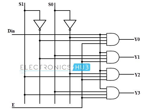
- Inputs:
$1$ | Outputs:$4$ | Select-Lines:$2$ (because$4=2^2$ ) - Truth-Table (Select Lines):
$S_1$ $S_0$ $O_0$ $O_1$ $O_2$ $O_3$ 0 0 I 0 0 0 0 1 0 I 0 0 1 0 0 0 I 0 1 1 0 0 0 I - SoP:
$\bar S_1 \bar S_0 O_1,\ \bar S_1 S_0 O_2 ,\ S_1 \bar S_0 O_3,\ S_1 S_0 O_4$ - Logic Diagram:
- Select Lines:
$S_1$ ,$S_0$ - Inputs:
$D$ - Output:
$Y_0$ ,$Y_1$ ,$Y_2$ ,$Y_3$ 
Image taken from here
- Select Lines:

- It is a multi-input multi-output device.
- Inputs:
$n$ | Outputs: upto$2^n$ - Applications:
- Binary to Octal (3:8)
- Binary to Hexadecimel (4:16)
- Binary to Decimel (4:10)
- Truth-Table (3:8 Decoder):
X Y Z $D_0$ $D_1$ $D_2$ $D_3$ $D_4$ $D_5$ $D_6$ $D_7$ 0 0 0 1 0 0 0 0 0 0 0 0 0 1 0 1 0 0 0 0 0 0 0 1 0 0 0 1 0 0 0 0 0 0 1 1 0 0 0 1 0 0 0 0 1 0 0 0 0 0 0 1 0 0 0 1 0 1 0 0 0 0 0 1 0 0 1 1 0 0 0 0 0 0 0 1 0 1 1 1 0 0 0 0 0 0 0 1 - SoP:
$\bar X \bar Y \bar Z D_0 + \bar X \bar Y Z D_1 + \bar X Y \bar Z D_2 + \bar X Y Z D_3 + X \bar Y \bar Z D_4 + X \bar Y Z D_5 + X Y \bar Z D_6 + X Y Z D_7$
- It is a multi-input multi-output device.
- Inputs:
$2^n$ | Outputs: upto$n$ - Applications:
- Octal to Binary (8:3)
- Hexadecimel to Binary (16:4)
- Decimel to Binary (10:4)
- Truth-Table (8:3 Encoder):
$E_0$ $E_1$ $E_2$ $E_3$ $E_4$ $E_5$ $E_6$ $E_7$ X Y Z 1 0 0 0 0 0 0 0 0 0 0 0 1 0 0 0 0 0 0 0 0 1 0 0 1 0 0 0 0 0 0 1 0 0 0 0 1 0 0 0 0 0 1 1 0 0 0 0 1 0 0 0 1 0 0 0 0 0 0 0 1 0 0 1 0 1 0 0 0 0 0 0 1 0 1 1 0 0 0 0 0 0 0 0 1 1 1 1 - SoP:
$\bar X \bar Y \bar Z E_0 + \bar X \bar Y Z E_1 + \bar X Y \bar Z E_2 + \bar X Y Z E_3 + X \bar Y \bar Z E_4 + X \bar Y Z E_5 + X Y \bar Z E_6 + X Y Z E_7$
- Example, Inputs:
$4=2^2$ and Output:$2$ - V: Valid
- Truth Table:
$I_3$ $I_2$ $I_1$ $I_0$ $O_1$ $O_0$ $V$ 0 0 0 0 x x 0 0 0 0 1 0 0 1 0 0 1 0 0 1 1 0 1 0 0 1 0 1 1 0 0 0 1 1 1 - In this type of encoder, there's no output (
$V=0$ ), if all the inputs are$0$ . - For a normal encoder, the output is the same for inputs
$0,0,0,0$ &$1,0,0,0$ ie$I_3=1$ , while the rest are 0. So, in a Priority encoder, we have an extra output$V$ , and the outputs are valid only when$V=1$ . - If 2 inputs become 1, no problems arise because the inputs are considered based on priority. Assuming that
$I_3>I_2>I_1>I_0$ , if$I_2=1$ &$I_1=1$ , only$I_2$ will be considered.
- Consists of a memory element that stores the present output.
- Output not only depends on the input, but also on the previous output.
- Inputs:
$I$ (Input) |$Q_n$ (Present output) - Output:
$Q_{n+1}$ (Next Output)
- For Latches, the output depends on the Gate used to design it.
- Inputs:
$S$ (Set),$R$ (Reset) | Outputs:$Q_{n+1} / Q$ ,$\bar Q$ - Property of NAND Gate: If any 1 of the inputs is 0, output is 1.
- Truth-Table:
$S$ $R$ $Q_{n+1}$ ($Q$ )0 0 Invalid 0 1 1 1 0 0 1 1 Hold / Q - Inputs:
$S=0$ ,$R=0$ | Outputs:$Q=1$ ,$\bar Q=1$ - NAND Gate (I) will output 1, since one of the inputs is 0.
- NAND Gate (II) will output 1, since one of the inputs is 0.
- This is invalid since the outputs should've been complimentary to each other.
- Circuit-Diagram:

- Inputs:
$S=0$ ,$R=1$ | Outputs:$Q=1$ ,$\bar Q=0$ - NAND Gate (I) will output 1, since one of the inputs is 0.
- NAND Gate (II) will output 0, since both the inputs are 1.
- Circuit-Diagram:

- Inputs:
$S=1$ ,$R=0$ | Outputs:$Q=0$ ,$\bar Q=1$ - NAND Gate (II) will output 1, since one of the inputs is 0.
- NAND Gate (I) will output 0, since both the inputs are 1.
- Circuit-Diagram:

- Inputs:
$S=1$ ,$R=1$ | Outputs:$Q=Q$ ,$\bar Q=\bar Q$ - Circuit-Diagram:

- NAND Gate (II) will always output
$\bar Q$ , which will be taken as an input to NAND Gate (I). - Also, NAND Gate (I) will always output
$Q$ , which will be taken as an input to NAND Gate (II). - So, for NAND Gate (I), output:
$\bar {(1.\bar Q)}$ $\bar 1 . \bar {\bar Q}$ $0+Q$ $Q$
- Also, for NAND Gate (II), output:
$\bar {1.Q}$ $\bar 1 . \bar Q$ $0 + \bar Q$ $\bar Q$
- Circuit-Diagram:


- Inputs:
$S$ (Set),$R$ (Reset) | Outputs:$Q_{n+1} / Q$ ,$\bar Q$ - Property of NOR Gate: If any 1 of the inputs is 1, output is 0.
- Truth-Table:
$S$ $R$ $Q_{n+1}$ ($Q$ )0 0 Hold / Q 0 1 0 1 0 1 1 1 Invalid - Inputs:
$S=0$ ,$R=0$ | Outputs:$Q=Q$ ,$\bar Q=\bar Q$ - Circuit-Diagram:

- NOR Gate (II) will always output
$Q$ , which will be taken as an input to NOR Gate (I). - Also, NOR Gate (I) will always output
$\bar Q$ , which will be taken as an input to NOR Gate (II). - So, for NOR Gate (II), output:
$\bar {0+\bar Q}$ $\bar 0.\bar {\bar Q}$ $1.Q$ $Q$
- Also, for NAND Gate (I), output:
$\bar {0+Q}$ $\bar 0. \bar Q$ $1.\bar Q$ $\bar Q$
- Circuit-Diagram:
- Inputs:
$S=0$ ,$R=1$ | Outputs:$Q=0$ ,$\bar Q=1$ - NOR Gate (II) will output 0, since one of the inputs is 1.
- NOR Gate (I) will output 1, since both the inputs are 0.
- Circuit-Diagram:

- Inputs:
$S=1$ ,$R=0$ | Outputs:$Q=1$ ,$\bar Q=0$ - NOR Gate (I) will output 0, since one of the inputs is 1.
- NOR Gate (II) will output 1, since both the inputs are 0.
- Circuit-Diagram:

- Inputs:
$S=1$ ,$R=1$ | Outputs:$Q=0$ ,$\bar Q=0$ - NAND Gate (I) will output 0, since one of the inputs is 1.
- NAND Gate (II) will output 0, since one of the inputs is 1.
- This is invalid since the outputs should've been complimentary to each other.
- Circuit-Diagram:


- A Flip-Flop only works when the Clock is triggered.
- The SR Flip-Flop is the most basic version of Flip-Flops, all other Flip-Flops are designed from it.
- For Flip-Flops, the output is same regardless of the Gate used to design it.
- Flip-Flops also have 2 more pins, clear and preset.
- Clear: Force
0as output. - Preset: Force
1as output. - Low / High enabled flip-flop: The pins get enabled when the input for Clear/Preset is low/high.
- Notation:

- Clear: Force

- Inputs:
$S$ ,$R$ | Outputs:$Q_{n}$ ,$\bar Q_n$ - Property of NAND Gate: If any 1 of the inputs is 0, output is 1.
- When the Clock is triggered, value
1is passed to both NAND Gates. - Truth-Table:
$CLK$ $S$ $R$ $Q_{n}$ 0 Any Any Q / Hold 1 0 0 Q / Hold 1 0 1 0 / Reset 1 1 0 1 / Set 1 1 1 Invalid - Inputs:
$S=0$ ,$R=0$ | Outputs:$Q_n=Q$ ,$\bar Q_n=\bar Q$ - Circuit-Diagram:

- Circuit-Diagram:
- Inputs:
$S=0$ ,$R=1$ | Outputs:$Q_n=0$ ,$\bar Q_n=1$ - Circuit-Diagram:

- Circuit-Diagram:
- Inputs:
$S=1$ ,$R=0$ | Outputs:$Q_n=1$ ,$\bar Q_n=0$ - Circuit-Diagram:

- Circuit-Diagram:
- Inputs:
$S=1$ ,$R=1$ | Outputs:$Q_n=1$ ,$\bar Q_n=1$ - Circuit-Diagram:

- Circuit-Diagram:


- We use AND Gate instead of NOR Gate, as inputs to the Latch. This is because, if we use NOR Gates, they'll always output
0when the clock is triggered (Property of NOR Gate: If any 1 of the inputs is 1, output is 0). So the Flip-Flop will not work properly. - When the Clock is triggered, value
1is passed to both NOR Gates. - Truth-Table:
$CLK$ $S$ $R$ $Q_n$ 0 Any Any Q / Hold 1 0 0 Q / Hold 1 0 1 0 / Reset 1 1 0 1 / Set 1 1 1 0 / Invalid - Inputs:
$S=0$ ,$R=0$ | Outputs:$Q_n=Q$ ,$\bar Q_n=\bar Q$ - Circuit-Diagram:

- Circuit-Diagram:
- Inputs:
$S=0$ ,$R=1$ | Outputs:$Q_n=0$ ,$\bar Q_n=1$ - Circuit-Diagram:

- Circuit-Diagram:
- Inputs:
$S=1$ ,$R=0$ | Outputs:$Q_n=1$ ,$\bar Q_n=0$ - Circuit-Diagram:

- Circuit-Diagram:
- Inputs:
$S=1$ ,$R=1$ | Outputs:$Q_n=0$ ,$\bar Q_n=0$ - Circuit-Diagram:

- Circuit-Diagram:


- SR Flip-Flop Truth-Table:
$CLK$ $S$ $R$ $Q_n$ 0 Any Any Hold 1 0 0 Q / Hold 1 0 1 0 / Reset 1 1 0 1 / Set 1 1 1 0 / Invalid -
Characteristic Table:
- Inputs: 3 {$S$,$R$,$Q_n$} | Outputs: 1, {$Q_{n+1}$}
-
Corresponds to:- If
$Q_n$ is inHoldstate,$Q_{n+1}$ will be same as$Q_n$ - If
$Q_n$ is inResetstate,$Q_{n+1}$ will$0$ regardless of the value of$Q_n$ - If
$Q_n$ is inSetstate,$Q_{n+1}$ will$1$ regardless of the value of$Q_n$ - If
$Q_n$ is ininvalidstate,$Q_{n+1}$ will also be invalid.
- If
- Truth-Table (x: don't care):
$S$ $R$ $Q_n$ $Q_{n+1}$ Corresponds to 0 0 0 0 Hold 0 0 1 1 Hold 0 1 0 0 Reset 0 1 1 0 Reset 1 0 0 1 Set 1 0 1 1 Set 1 1 0 x Invalid 1 1 1 x Invalid - SoP (based on
$Q_{n+1}$ ):$\bar S \bar R Q_{n} + S \bar R \bar Q_{n} + S \bar R Q_{n} + S R \bar Q_{n} + S R Q_{n}$ - K-Map:
$↓S\ |\ R {Q_n}→$ $\bar R \bar {Q_n}_{(00)}$ $\bar R {Q_n}_{(01)}$ $R {Q_n}_{(11)}$ $R \bar {Q_n}_{(10)}$ $\bar S_{(0)}$ $null_{(0)}$ $1_{(1)}$ $null_{(3)}$ $null_{(2)}$ $S_{(1)}$ $1_{(4)}$ $1_{(5)}$ $d_{(7)}$ $d_{(6)}$ - Pairs:
${1,5},{4,5,7,6}$ - Min-Terms: 2 ie
$S + \bar R Q_{n}$
- Pairs:
-
Excitation Table:
- Represents corresponding inputs to outputs
$Q_n$ &$Q_{n+1}$ - Prerequisite:
Characteristic Table - Truth-Table (x: don't care / cannot be determined):
$Q_n$ $Q_{n+1}$ $S$ $R$ 0 0 0 x 0 1 1 0 1 0 0 1 1 1 x 0
- Represents corresponding inputs to outputs

- Inputs:
$J$ ,$K$ | Outputs:$Q_{n}$ ,$\bar Q_n$ - Property of NAND Gate: If any 1 of the inputs is 0, output is 1.
- When the Clock is triggered, value
1is passed to both NAND Gates. - Truth-Table:
$CLK$ $S$ $R$ $Q_{n+1}$ ($Q$ )0 Any Any Q / Hold 1 0 0 Q / Hold 1 0 1 0 / Reset 1 1 0 1 / Set 1 1 0/1 Toggle - Inputs:
$J=0$ ,$K=0$ | Outputs:$Q_n=Q$ ,$\bar Q_n=\bar Q$ - Inputs:
$J=0$ ,$K=1$ | Outputs:$Q_n=0$ ,$\bar Q_n=1$ - Inputs:
$K=1$ ,$K=0$ | Outputs:$Q_n=1$ ,$\bar Q_n=0$ - Inputs:
$J=1$ ,$K=1$ | Outputs if$Q_n=1$ ,$\bar Q_n=0$ are$Q_{n+1}=0$ ,$\bar Q_{n+1}=1$ - Let
$Q_n=1$ , then$\bar Q_{n}=0$ . -
$Q_{n}=1$ goes as input to NAND Gate$K$ . It outputs$1$ -
$\bar Q_n=0$ goes as input to NAND Gate$J$ . It outputs$0$ . - The SR Latch gets input
$1,0$ and outputs$Q_{n+1}=0$ ,$\bar Q_{n+1}=1$ .
- Let
- Inputs:
$J=1$ ,$K=1$ | Outputs if$Q_n=0$ ,$\bar Q_n=1$ are$Q_{n+1}=1$ ,$\bar Q_{n+1}=0$ - Let
$Q_n=0$ , then$\bar Q_{n}=1$ . -
$Q_{n}=0$ goes as input to NAND Gate$J$ . It outputs$0$ -
$\bar Q_n=1$ goes as input to NAND Gate$K$ . It outputs$1$ . - The SR Latch gets input
$0,1$ and outputs$Q_{n+1}=1$ ,$\bar Q_{n+1}=0$ .
- Let


- SR Flip-Flop Truth-Table:
$CLK$ $S$ $R$ $Q_n$ 0 Any Any Q / Hold 1 0 0 Q / Hold 1 0 1 0 / Reset 1 1 0 1 / Set 1 1 1 Toggle -
Characteristic Table:
- Inputs: 3 {$J$,$K$,$Q_n$} | Outputs: 1, {$Q_{n+1}$}
-
Corresponds to:- If
$Q_n$ is inHoldstate,$Q_{n+1}$ will be same as$Q_n$ - If
$Q_n$ is inResetstate,$Q_{n+1}$ will$0$ regardless of the value of$Q_n$ - If
$Q_n$ is inSetstate,$Q_{n+1}$ will$1$ regardless of the value of$Q_n$ - If
$Q_n$ is inTogglestate,$Q_{n+1}$ will be the opposite of$Q_n$ .
- If
- Truth-Table:
$J$ $K$ $Q_n$ $Q_{n+1}$ Corresponds to 0 0 0 0 Hold 0 0 1 1 Hold 0 1 0 0 Reset 0 1 1 0 Reset 1 0 0 1 Set 1 0 1 1 Set 1 1 0 1 Toggle 1 1 1 0 Toggle - SoP:
$\bar J \bar K Q_{n} + J \bar K \bar Q_n + J \bar K Q_n + J K \bar Q_n$ - K-Map:
$↓J\ |\ K {Q_n}→$ $\bar K \bar {Q_n}_{(00)}$ $\bar K {Q_n}_{(01)}$ $K {Q_n}_{(11)}$ $K \bar {Q_n}_{(10)}$ $\bar J_{(0)}$ $null_{(0)}$ $1_{(1)}$ $null_{(3)}$ $null_{(2)}$ $J_{(1)}$ $1_{(4)}$ $1_{(5)}$ $null_{(7)}$ $1_{(6)}$ - Pairs:
${1,5},{4,6}$ - Min-Terms: 2 ie
$\bar K Q_n + J \bar Q_{n}$
- Pairs:
-
Excitation Table:
- Represents corresponding inputs to outputs
$Q_n$ &$Q_{n+1}$ - Prerequisite:
Characteristic Table - Truth-Table (x: cannot be determined):
$Q_n$ $Q_{n+1}$ $J$ $K$ 0 0 0 x 0 1 1 x 1 0 x 1 1 1 x 0
- Represents corresponding inputs to outputs
-
T: Time duration of 1 clock pulse, consisting of 1 low & 1 high.
-
Level Trigger
- Low Level Trigger: when
$clock=0$ - High Level Trigger: when
$clock=1$ $T_w=T/2$
- Low Level Trigger: when
-
Edge Trigger
- Positive Edge Trigger: When clock switches from
$0$ to$1$ - Negative Edge Trigger: When clock switches from
$1$ to$0$ 
- Positive Edge Trigger: When clock switches from
-
Representation:
- Remember the edge cases in the right-most representation(s).

- Remember the edge cases in the right-most representation(s).


Requirements (all are mandatory):
- Level Triggered JK Flip-Flop.
- Inputs:
$J=1$ ,$K=1$ (Toggle Mode) -
$T_w \gt \gt T_d$ $T_w$ : Time duration that clock stays at a particular state
$T_d$ : Time taken by the Flip-Flop to process the inputs
What happens:
- We know that JK Flip-Flop gives next state
$Q_n=1$ for current state$Q_n=0$ . - If the clock stays at the same state
$CLK=1$ for a sufficiently long time ($T_w \gt \gt T_d$ ), the outputs will get fed back to the Flip-Flop, and toggle the inputs again. - This will keep happening again and again, and we will not be able to figure out the output of the Flip-Flop. This is known as Race Condition.


- This is a solution for Race Around Condition in a JK Flip-Flop.

- The feedback from the Slave Flip-Flop goes to the Master Flip-Flop.
- The clock triggers only the Master Flip-Flop, and not the Slave Flip-Flop.
- The Master Flip-Flop is giving the desired output, and the Slave Flip-Flop is forwarding it as-is.

- Inputs: 2:
${D,CLK}$ | Outputs: 2:${Q_n,\bar Q_n}$ - Also known as
transparent latchorstorage device. - Truth Table:
$D$ $Q_{n}$ 0 0 1 1
Construction using SR Flip-Flop:
- Input:
$D=0$ | Outputs:$Q_n=0$ ,$\bar Q_n=1$ - Circuit-diagram:

- Circuit-diagram:
- Input:
$D=1$ | Outputs:$Q_n=1$ ,$\bar Q_n=0$ - Circuit-diagram:

- Circuit-diagram:


-
Characteristic Table:
- Inputs: 2
${D,Q_n}$ | Outputs: 1,${Q_{n+1}}$ $D$ $Q_n$ $Q_{n+1}$ 0 0 0 0 1 0 1 0 1 1 1 1 - Output is same as the input.
- Inputs: 2
-
Excitation Table:
- Inputs: 2
${Q_n,Q_{n+1}}$ | Outputs: 1,${D}$ $Q_n$ $Q_{n+1}$ D 0 0 0 0 1 1 1 0 0 1 1 1
- Inputs: 2
- Inputs: 2:
${T,CLK}$ | Outputs: 2:${Q_n,\bar Q_n}$ - If
$T=0$ , outputs the same value as current input. - If
$T=1$ , outputs the complement of current input. - Truth Table:
$T$ $Q_{n}$ 0 $Q_n$ 1 $\bar Q_n$ - Input:
$T$ | Outputs:$Q_n$ ,$\bar Q_n$ - Logic-diagram:

- Logic-diagram:

-
Characteristic Table:
- Inputs: 2
${Y,Q_n}$ | Outputs: 1,${Q_{n+1}}$ $T$ $Q_n$ $Q_{n+1}$ 0 0 0 0 1 1 1 0 1 1 1 0 - Output:
$Q_{n+1}=T⊕Q_n$
- Inputs: 2
-
Excitation Table:
- Inputs: 2
${Q_n,Q_{n+1}}$ | Outputs: 1,${T}$ $Q_n$ $Q_{n+1}$ T 0 0 0 0 1 1 1 0 1 1 1 0
- Inputs: 2
- We need to excite SR Flip-Flop, so it gets the Characteristics of D Flip-Flop.
- First, we define the Characteristics of D Flip-Flop.
- Next, we need the Excitation Table of SR Flip-Flop.
- Merge the Excitation Table of SR Flip-Flop, with the Characteristic Table of D Flip-Flop.
D $Q_n$ $Q_{n+1}$ $S$ $R$ 0 0 0 0 x 0 1 0 0 1 1 0 1 1 0 1 1 1 x 0 - Generate K-Map for
$S$ :$↓D\ |\ {Q_n}→$ $\bar {Q_n}_{(00)}$ ${Q_n}_{(01)}$ $\bar D_{(0)}$ $null_{(0)}$ $null_{(1)}$ $D_{(1)}$ $1_{(2)}$ $x_{(3)}$ - Pairs:
${2,3}$ - Min-Terms: 1 ie
$D$
- Pairs:
- Generate K-Map for
$R$ :$↓D\ |\ {Q_n}→$ $\bar {Q_n}_{(00)}$ ${Q_n}_{(01)}$ $\bar D_{(0)}$ $x_{(0)}$ $1_{(1)}$ $D_{(1)}$ $null_{(2)}$ $null_{(3)}$ - Pairs:
${0,1}$ - Min-Terms: 1 ie
$\bar D$ - Logic-diagram:

- Pairs:

- We need to excite T Flip-Flop, so it gets the Characteristics of JK Flip-Flop.
- First, we define the Characteristics of JK Flip-Flop.
- Next, we need the Excitation Table of T Flip-Flop.
- Merge the Excitation Table of T Flip-Flop, with the Characteristic Table of JK Flip-Flop.
J K $Q_n$ $Q_{n+1}$ T 0 0 0 0 0 0 0 1 1 0 0 1 0 0 0 0 1 1 0 1 1 0 0 1 1 1 0 1 1 0 1 1 0 1 1 1 1 1 0 1 - K-Map for
$T$ :$↓J\ |\ K {Q_n}→$ $\bar K \bar {Q_n}_{(00)}$ $\bar K {Q_n}_{(01)}$ $K {Q_n}_{(11)}$ $K \bar {Q_n}_{(10)}$ $\bar J_{(0)}$ $null_{(0)}$ $null_{(1)}$ $1_{(3)}$ $null_{(2)}$ $J_{(1)}$ $1_{(4)}$ $null_{(5)}$ $1_{(7)}$ $1_{(6)}$ - Pairs:
${3,7},{4,6}$ - Min-Terms: 2 ie
$K Q_n + J \bar Q_{n}$ - Logic-diagram:

- Pairs:

- We need to excite SR Flip-Flop so it gets the Characteristics of JK Flip-Flop.
- First, we define the Characteristics of JK Flip-Flop.
- Next, we need the Excitation Table of SR Flip-Flop.
- Merge the Excitation Table of SR Flip-Flop, with the Characteristic Table of JK Flip-Flop.
$J$ $K$ $Q_n$ $Q_{n+1}$ $S$ $R$ 0 0 0 0 0 x 0 0 1 1 x 0 0 1 0 0 0 x 0 1 1 0 0 1 1 0 0 1 1 0 1 0 1 1 x 0 1 1 0 1 1 0 1 1 1 0 0 1 - K-Map for
$S$ :$↓J\ |\ K {Q_n}→$ $\bar K \bar {Q_n}_{(00)}$ $\bar K {Q_n}_{(01)}$ $K {Q_n}_{(11)}$ $K \bar {Q_n}_{(10)}$ $\bar J_{(0)}$ $null_{(0)}$ $x_{(1)}$ $null_{(3)}$ $null_{(2)}$ $J_{(1)}$ $1_{(4)}$ $x_{(5)}$ $null_{(7)}$ $1_{(6)}$ - Pairs:
${4,6}$ - Min-Terms: 1 ie
$J \bar Q_{n}$
- Pairs:
- K-Map for
$R$ :$↓J\ |\ K {Q_n}→$ $\bar K \bar {Q_n}_{(00)}$ $\bar K {Q_n}_{(01)}$ $K {Q_n}_{(11)}$ $K \bar {Q_n}_{(10)}$ $\bar J_{(0)}$ $x_{(0)}$ $null_{(1)}$ $1_{(3)}$ $x_{(2)}$ $J_{(1)}$ $null_{(4)}$ $null_{(5)}$ $1_{(7)}$ $null_{(6)}$ - Pairs:
${3,7}$ - Min-Terms: 1 ie
$K Q_{n}$ 
- Pairs:

- We need to excite JK Flip-Flop so it gets the Characteristics of SR Flip-Flop.
- First, we define the Characteristics of SR Flip-Flop.
- Next, we need the Excitation Table of JK Flip-Flop.
- Merge the Excitation Table JK Flip-Flop, with the Characteristic Table of SR Flip-Flop.
$S$ $R$ $Q_n$ $Q_{n+1}$ $J$ $K$ 0 0 0 0 0 x 0 0 1 1 x 0 0 1 0 0 0 x 0 1 1 0 x 1 1 0 0 1 1 x 1 0 1 1 x 0 1 1 0 x x x 1 1 1 x x x - K-Map for
$J$ :$↓S\ |\ K {Q_n}→$ $\bar K \bar {Q_n}_{(00)}$ $\bar K {Q_n}_{(01)}$ $K {Q_n}_{(11)}$ $K \bar {Q_n}_{(10)}$ $\bar S_{(0)}$ $null_{(0)}$ $x_{(1)}$ $x_{(3)}$ $null_{(2)}$ $S_{(1)}$ $1_{(4)}$ $x_{(5)}$ $x_{(7)}$ $x_{(6)}$ - Pairs:
${4,5,7,6}$ - Min-Terms: 1 ie
$S$
- Pairs:
- K-Map for
$K$ :$↓J\ |\ K {Q_n}→$ $\bar K \bar {Q_n}_{(00)}$ $\bar K {Q_n}_{(01)}$ $K {Q_n}_{(11)}$ $K \bar {Q_n}_{(10)}$ $\bar S_{(0)}$ $null_{(0)}$ $null_{(1)}$ $1_{(3)}$ $x_{(2)}$ $S_{(1)}$ $x_{(4)}$ $null_{(5)}$ $x_{(7)}$ $x_{(6)}$ - Pairs:
${3,2,7,6}$ - Min-Terms: 1 ie
$R$ 
- Pairs:

- A counter is a device that stores and sometimes displays the number of times a particular event or process has occured.
- Counters count clock pulses.
- They are usually constructed of a number of flip-flops connected in cascade.
- We only use edge-triggered flip-flops, not level triggered flip-flops because of race condition of level triggered flip-flops.
- For a 0-1-2-3-4-0 ... etc, counter, it counts from 0 to 1,2,3,4, then comes back to 0. There are a total of 5 states {0,1,2,3,4}, and it is a Mod-5 counter.
- The counter moves to the next state everytime a clock pulse is applied to it.
- Consequently, after every 5 clock pulses, it will come back to
0, if0is thestarting state. - After 21 clock pulses, it'll will be 1 state ahead of the
starting state, ie at1.
- To design a
Mod-5counter, we need$n$ Flip-Flops, such that$2^n \geq M$ . For$M=5$ ,$2^3 \geq 5$ , so we need$3$ Flip-Flops. - If the counter sequence is 0-1-4-8-5, then it is a
Mod-5counter. We should need$3$ Flip-Flops. However, we also need to look at the maximum number in the sequence, which is$8$ . To represent$8=1000$ , we would need$4$ Flip-Flops. So, when a counter sequence is given, check both the number of states and the largest value in the sequence. - Types of Counters:
Synchronous (+)&Asynchronous (-)+ All clocks are externally triggered. - The 1st clock is externally triggered. The 2nd clock is triggered by the output of the first flip-flop, the 3rd one gets triggered by the output of 2nd flip-flop ... and so on. + We can design both sequential and non-sequential circuits (like 0-3-2-6-4). - We can only design Sequential circuits like 0-1-2-3 (UP Sequential) or 3-2-1-0 (DOWN Sequential). + It is faster. - It is comparatively slower. + If we want to disable some flip-flops, we have to use extra Gates, which increases the complexity. - It is relatively simpler. + Example: Ring, Twisted Ring Counter - Example: Ripple Counter


- Design a Synchronous Counter using D Flip-Flop: 0-1-3-2
- Number of states:
$4$ , Largest number:$3$ .$2^2=4$ , and$3=11$ , so we need 2 Flip-Flops. - Current inputs:
$Q_1$ ,$Q_0$ - Next inputs:
$Q^+_1$ ,$Q^+_0$ - Representational inputs to the D Flip-Flops:
$D_1$ ,$D_0$ - Steps:
$Q_1$ $Q_0$ $Q^+_1$ $Q^+_0$ $D_1$ $D_0$ 0 0 0 1 0 1 0 1 1 1 1 1 1 0 0 0 0 0 1 1 1 0 1 0 - Write the current inputs.
- For each input, write the next state by looking at the sequence (0-1-3-2).
- From the Excitation Table of the D Flip-Flop, write the D states:
-
$D_1$ : Corresponds to$Q_1$ &$Q^+_1$ -
$D_0$ : Corresponds to$Q_0$ &$Q^+_0$
-
- Generate the Flip-Flop for
$D_1$ , using theCurrent Inputs$Q_1$ ,$Q_0$ .$↓Q_1\ |\ Q_0 →$ $\bar Q_0$ $Q_0$ $\bar Q_1$ $null_{(0)}$ $1_{(1)}$ $Q_1$ $null_{(2)}$ $1_{(3)}$ - Pairs:
${1,3}$ , Min-term:$Q_0$
- Pairs:
- Generate the Flip-Flop for
$D_0$ , using theCurrent Inputs$Q_1$ ,$Q_0$ .$↓Q_1\ |\ Q_0 →$ $\bar Q_0$ $Q_0$ $\bar Q_1$ $1_{(0)}$ $1_{(1)}$ $Q_1$ $null_{(2)}$ $null_{(3)}$ - Pairs:
${0,1}$ , Min-term:$\bar Q_1$
- Pairs:
- Logic Diagram:

- Number of states:

- In Asynchronous counter, we can identify if it is an UP or DOWN counter, from it's representation.
$Q$ &$\bar Q$ are the outputs used to trigger the clocks, and the arrows represent the clocks themselves.

- Type: Synchronous
- In an
n-bitring counter, out of$2^n$ states, there arenusable states, while the rest are not usable. - After
nclock cycles, it returns to it's starting position. - States for
4-bitCounter:$Q_3$ $Q_2$ $Q_1$ $Q_0$ 1 0 0 0 0 1 0 0 0 0 1 0 0 0 0 1 1 0 0 0 - After
4clock cycles, the counter returns back to it's starting position. - In a
4-bitring counter,- There are
$2^4=16$ states. - There are 4 usable states:
$1010, 0100, 0010, 0001$ . - It will be called a
Mod-4 Ring Counter.
- There are

- aka Johnson Counter
- Type: Synchronous
- In an
n-bitring counter, out of$2^n$ states, there are2nusable states, while the rest are not usable. - After
2nclock cycles, it returns to it's starting position. - States for
4-bitCounter:$Q_3$ $Q_2$ $Q_1$ $Q_0$ 0 0 0 0 0 1 0 0 1 1 0 0 1 1 1 0 1 1 1 1 0 1 1 1 0 0 1 1 0 0 0 1 0 0 0 0 - After
8clock cycles, the counter returns back to it's starting position. - In a
4-bitTwisted Ring counter,- There are
$2^4=16$ states. - There are 8 usable states:
$0000,0100,1100,1110,1111,0111,0011,0001,0000$ - It will be called a
Mod-4 Twisted Ring Counter.
- There are

- Type: Synchronous
- They are used to implement arithmetic operations: multiplication & division.
- D Flip-Flops are used for making Shift Registers.
- Left-Shift (for multiplication):
- 0 0 0 1 = 1
- 0 0 1 0 = 2 = 1*2
- 0 1 0 0 = 4 = 2*2
- 1 0 0 0 = 8 = 4*2
- Right-Shift (for division):
- 1 0 0 0 = 8
- 0 1 0 0 = 4 = 8/2
- 0 0 1 0 = 2 = 4/2
- 0 0 0 1 = 1 = 2/2
- 4 types of shift registers:
- SISO (Serial-In Serial-Out)

- SIPO (Serial-In Parallel-Out)

- PISO (Parallel-In Serial-Out)

- PIPO (Parallel-In Parallel-Out)

- SISO (Serial-In Serial-Out)
- Number of clock cycles needed for n-shift register:
Mode Loading Reading Total SISO n n-1 2n-1 SIPO n 0 n PISO 1 n-1 n PIPO 1 0 1 - Example 0:

- After 6 clock cycles, the value will be
$1,1,1,1$ when initial value is$0,1,1,0$ . - Outputs:
Clocks $Q_3$ $Q_2$ $Q_1$ $Q_0$ $C_0$ 0 1 1 0 $C_1$ 1 0 1 1 $C_2$ 0 1 0 1 $C_3$ 1 0 1 0 $C_4$ 1 1 0 1 $C_5$ 1 1 1 0 $C_6$ 1 1 1 1
- After 6 clock cycles, the value will be


- Formulae
- Table:
USM SM 1's 2's 0 000 +0 +0 +0 1 001 +1 +1 +1 2 010 +2 +2 +2 3 011 +3 +3 +3 4 100 -0 -3 -4 5 101 -1 -2 -3 6 110 -2 -1 -2 7 111 -3 -0 -1 - Explanation:
- Unsigned Magnitude (USM): Self-explanatory.
- Signed Magnitude (SM): In
$010$ , 0/1: +ve/-ve number, while$10=2$ in integer form. In$110$ , it will be$-2$ . - 1's Complement: Positive numbers (starting with 0) remain the same. For
$110$ , 1: -ve number, 1 becomes 0, and 0 becomes 1. So the result is$101$ , which is$-1$ . - 2's Complement: Positive numbers (starting with 0) remain the same. For
$110$ , $-12^{2}+12^{1}+0*2^{0}=-4+2=-2$. Note the$-$ sign for the 1st element, because the number is negative.
- For Signed Magniture (SM) & 1's Complement: For n-bits, there are
$2^n$ possible numbers, and the ranges are$-(2^{n-1}-1)$ to$(2^{n-1}-1)$ If Range is
$0$ to$2^n/2 - 1$ , then$2^n/2-1=2^{n}.2^{-1}-1=2^{n-1}-1$ - For 2's Complement: For n-bits, there are
$2^n$ possible numbers, and the ranges are$-(2^{n-1})$ to$(2^{n-1}-1)$ The negative range starts at one less than the previous, while the positive range remains the same.
- Example 0:
$1110+1100=11010$ , ie$14+12=26$ -
$1+1=10$ , carry$1$ .$1+1+1=11$ , carry$1$ .
-
- Example 1:
$1110.110+1100.011=11011.001$ , ie$14.750+12.375=27.125$
- Example 0:
$1110-0101=1001$ , ie$14-5=9$ -
$0-1=10-1=1$ , borrow$1$ .
-
- Example 1:
$1100-0101=0111$ , ie$12-5=7$ - In
$1100$ , right-most 0 needs 1. It can't get it from the position 3 element. So, it gets it from the position 2 element. - Position 2 element (1) will only give 10 to position 3 element (0).
- Again, position 3 element gives 1 to position 4 element.
- However,position 4 element gets 10 too, not 1.
- So,
$10-1=1$ ,$1-0=1$ ,$0-1=10-1=1$ , borrow$1$ .$0-0=0$ .
- Whenever we borrow
$1$ from a digit$1$ , all the 0's on the right get$1$ , but the right-most$0$ gets$10$ .
- In
- Example 2:
$11000-00001=10111$ , ie$24-1=23$ - See previous
- Example 3:
$11000-01111=01001$ , ie$24-15=9$